+86-400-850-4050


Didn't find what you were looking for?
Consult a professional engineer immediately for your service


In recent years, with the requirement of lead-free in the electronics industry, the research on the interface reaction between Sn-based lead-free solders and substrates has increased significantly. In electronic products, copper is often used as the substrate material.
| Project Background
In recent years, with the requirement of lead-free in the electronics industry, the research on the interface reaction between Sn-based lead-free solders and substrates has increased significantly. In electronic products, copper is often used as the substrate material. The reaction at the interface between the solder and the copper substrate during welding and service is a research topic that has attracted extensive attention. Due to the relatively high content of Sn in SnAgCu lead-free solder and the relatively high welding temperature, the dissolution rate of Cu in the solder joint and the growth rate of the interfacial intermetallic compounds are much higher than those of SnPb-based solders. Relevant research shows that the morphology and growth of the intermetallic compounds between the solder joint and the metal contact have a very important impact on the initiation and development of solder joint defects and the reliability of electronic assemblies.
| Project Overview
1. Metals that can be soldered by tin-lead alloy solder (also known as solder), such as copper, nickel, gold, silver, etc. A thin layer of a compound similar to a "tin alloy" will be rapidly formed between the solder and the metal of the soldering pad at high temperatures.
2. This substance originates from the actions of mutual combination, infiltration, migration, and diffusion of tin atoms and the atoms of the metal to be soldered. A thin layer of "intermetallic compound" appears immediately after cooling and solidification, and it will gradually grow and thicken afterwards.
3. The aging degree of such substances is affected by the amount of mutual infiltration between tin atoms and base metal atoms, and several layers can be distinguished. All kinds of intermetallic compounds formed between the solder and the metal to be soldered are collectively referred to as IMC.
|
|
|
|
|
|
|
|
|
|
|
|
|
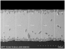
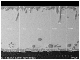
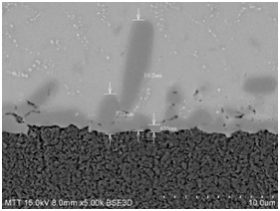
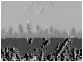
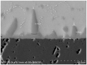
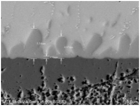
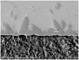
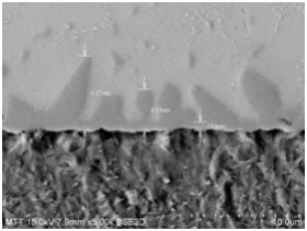
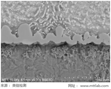
Figure 1. IMC test picture |
|
| Service Products / Fields
PCBA, PCB, FPC, etc.
| Testing Procedure
After cutting, inlaying, grinding, polishing, and micro-etching the sample, platinum is plated on the surface. Then, according to the standard operating procedure, the sample is placed in the sample chamber of the scanning electron microscope. The test position required by the customer is magnified for observation and measurement.
| Characteristics of IMC
(1) Its growth rate is proportional to temperature and is relatively slow at normal temperature.
(2) It is highly brittle and has poor ductility at room temperature, and is prone to breakage.
(3) Low density.
(4) High melting point.
| Influence of IMC on Soldering
Even a very thin layer of IMC can form a stable connection between the solder and the substrate. A thicker IMC can cause stress concentration at the interface under the action of thermal cycling, leading to brittle fracture and even relaxation of the entire solder body. The influence of IMC on soldering performance is very complex. The thicker the IMC, the more likely the solder joint is to fail in the thermal fatigue test. The main failure mode is fracture, and cracks usually occur at the interface between the IMC and the solder inside the solder joint.
Once a relatively thick IMC with a small spacing appears between the original molten tin layer or tin-sprayed layer of the pad and the base copper, it will greatly hinder subsequent soldering of the pad. That is, both the solderability and wettability will deteriorate.
| Formation and Growth Laws of IMC
The formation of the IMC at the SnAgCu interface is divided into two stages. The first stage is the IMC formed between the Cu substrate and the liquid solder during the soldering process, and the second stage is the IMC formed between the Cu substrate and the solid solder during the post-soldering service process. It is generally believed that the formation of IMC during the soldering process is a mechanism dominated by interfacial chemical reactions, and the evolution of IMC during the service process is a mechanism dominated by element diffusion. There are very obvious differences in the morphology and growth kinetics of the IMC in these two stages.
After the solder joint is formed, there are two kinds of intermetallic compounds, Cu6Sn5 and Cu3Sn, at the SnAgCu-Cu interface. Cu6Sn5 is located on the solder side, is relatively thick, and grows in a scallop shape into the liquid solder, resulting in a rough morphology at the boundary between the IMC and the solder. It is formed during the soldering process. Cu3Sn is located between the Cu substrate and Cu6Sn5, is relatively thin, and is formed during the service process.
During the soldering process, after the Cu substrate makes metallurgical contact with the liquid solder, solid Cu dissolves into the liquid solder, and a layer of saturated Cu is formed in the liquid solder adjacent to the Cu substrate. When the dissolution of Cu reaches a local equilibrium state, the IMC is formed here. The formation of Cu6Sn5 consumes the Cu in the saturated liquid solder. As Cu6Sn5 crystallizes and connects with each other, a continuous IMC layer is formed at the interface between the Cu substrate and the solder. This continuously distributed IMC blocks the path for the further dissolution of the Cu substrate into the liquid solder. Sn and Cu6Sn5 are in an equilibrium state, while the interface between the solid Cu and the Cu6Sn5 layer is in a non-equilibrium state. Once the temperature is high enough to activate the reaction between Cu atoms and Sn atoms, a more stable Cu3Sn will be formed at the interface between the Cu substrate and the Cu6Sn5 layer through solid-phase diffusion.
The IMC formed between the Cu substrate and the liquid solder during the welding process is mainly determined by the interfacial chemical reaction. Currently, there are no theories and methods that can describe the growth law of IMC in this process. During the service process after welding, the IMC formed between the Cu substrate and the solid solder is mainly dominated by element diffusion. Fick's diffusion law is applied to describe the growth law of IMC at this stage. The thickness of the IMC is L2 = Dt, where D is the diffusion coefficient and t is the diffusion time.
| How to Appropriately Control the IMC
The Au/Ni/Cu three-layer structure is a widely used pad structure in electronic packaging devices. The Au layer, as a protective film on the Ni surface, has good electrical conductivity, wettability, and corrosion resistance. The Ni layer has a very slow dissolution rate in the solder and can act as a barrier layer for the Cu layer to prevent the reaction between the substrate Cu and the solder.
In addition, in the electroless Ni plating process, the coating contains a certain amount of P element. Research has found that during the reflow soldering process, P does not dissolve into the solder, and a high-stress layer enriched with Ni, P, and Sn is formed between the Ni layer and the IMC layer. The content of P has a certain influence on the thickness of the IMC. When the P content in the coating is relatively high, the P-rich layer formed between the Ni layer and the IMC effectively prevents Ni from participating in the reaction, reduces the probability of IMC formation, and thus reduces the thickness of the IMC.

Maxin Testing Laboratory
Learn more about our company

Electronic Manufacturing Information Hub
See more exciting case studies

Video Channel
Watch more exciting videos


 Buildings A1, A3, and A5, Peking University Science and Innovation Park, Songbai Road, Bao'an District, ShenzhenBuilding 3, Xinyao Valley, 415 Changyang Street, Suzhou Industrial Park, Suzhou City1st Floor, Building 4, No. 39 Anzhi Street, Suzhou Industrial Park, Suzhou City