


 +86-400-850-4050


Didn't find what you were looking for?
Consult a professional engineer immediately for your service


Dimensional measurement in slice analysis is a key link connecting design, manufacturing, and reliability. Especially in high-end PCBs (such as IC carriers and high-frequency high-speed boards), micron-level deviations may directly affect signal integrity or thermomechanical reliability.
| Project Background
Dimensional measurement in slice analysis is a key link connecting design, manufacturing, and reliability. Especially in high-end PCBs (such as IC carriers and high-frequency high-speed boards), micron-level deviations may directly affect signal integrity or thermomechanical reliability. Combining destructive slicing with non-destructive testing (such as CT) can comprehensively evaluate product quality. In PCB (Printed Circuit Board) slice analysis, dimensional measurement is the core means to evaluate the quality of manufacturing processes, verify design compliance, and conduct fault analysis. Through the Cross-Section technology, the microscopic dimensions of the internal structure of the PCB can be visually observed and accurately measured.
| Project Overview
1. Purpose of the test
Design verification: Ensure that the actual PCB dimensions (such as line width and spacing) are consistent with the design documents (Gerber/CAD) to avoid electrical performance deviations caused by dimensional issues;
Process control: Monitor the stability of key processes such as etching, drilling, and electroplating (such as the uniformity of hole copper thickness);
Reliability assurance: Prevent assembly failures (such as insufficient tolerance of plug-in holes), signal integrity issues (impedance mismatch), or long-term failures (such as thermal expansion cracking) caused by dimensional out-of-tolerance;
Standard compliance: Meet industry standards such as IPC and ISO or customer-customized requirements (such as the Class 3 standard for automotive electronics).
2. Measuring object
|
测量参数 Measurement parameters |
典型要求 Typical requirements |
影响 Impact |
|
线宽/线距 Line width/Line spacing |
±10%设计值(高速板±5%) ±10% of the design value (±5% for high-speed boards) |
阻抗控制、电流承载能力 Impedance control, current carrying capacity |
|
孔铜厚度 Copper thickness of holes |
通孔≥25μm(Class 3) Through holes ≥25μm (Class 3) |
导电可靠性、机械强度 Conductive reliability, mechanical strength |
|
介质层厚度 Dielectric layer thickness |
±10%标称值 ±10% of the nominal value |
阻抗匹配、信号传输损耗 Impedance matching, signal transmission loss |
|
阻焊层开口 Solder mask opening |
偏移≤50μm Offset ≤ 50μm |
焊接良率(避免阻焊覆盖焊盘) Soldering yield (avoid solder mask covering bonding pads) |
|
板厚/翘曲度 Board thickness/warpage |
多层板±10%,翘曲≤0.7% ±10% for multilayer boards, warpage ≤ 0.7% |
装配兼容性、热机械应力 Assembly compatibility, thermomechanical stress |
|
表面处理层厚 Surface treatment layer thickness |
ENIG镍3-5μm,金0.05-0.1μm ENIG: nickel 3-5μm, gold 0.05-0.1μm |
焊接性、抗氧化性 Solderability, oxidation resistance |
3. Common measurement methods
(1) Non-destructive testing
X-ray inspection:
Principle: Penetrating imaging to detect hidden structures
Applications: Void in BGA solder joints, analysis of inner layer alignment, vertical filling rate of support holes.
(2) Destructive testing
Cross-Section analysis:
Steps: Sampling → Resin encapsulation → Grinding and polishing → Observation under microscope/SEM.
Applications: Measurement of hole copper thickness, interlayer structure, IMC layer (accuracy ±0.5μm).
| Test Objective
The ultimate goal of the PCB dimensional measurement test is closed-loop quality control:
Inspection: Quantify physical characteristics;
Analysis: Correlate process/design defects;
Improvement: Optimization of driving process or design iteration.
In high-end PCBs (such as 5G millimeter-wave antenna boards and AI server carrier boards), micron-level dimensional control directly determines the success or failure of the product. It is necessary to combine destructive (sectioning) and non-destructive (AOI/CT) means to achieve full-coverage inspection.
| Testing Standards
IPC-A-600 "Acceptability of PCBs"
IPC-6012 "Qualification and Performance Specification for Rigid PCBs"
IPC-TM-650 2.2.5A Test Method Manual: Cross-Section Dimensional Measurement
GB/T 16594-2008 General rules for measurement of length in micron scale by SEM
| Service Products / Fields
I. Consumer Electronics
Applied products: 1. Motherboards of smartphones/computers/tablets 2. Smart wearable devices (such as flexible circuits of TWS earphones) 3. Home appliance control boards
II. Communication Equipment
Applied products: 1. 5G base station AAU radio frequency boards; 2. PCB of optical modules; 3. Millimeter-wave antenna arrays
III. Automotive Electronics
Application products: 1. Engine Control Unit (ECU); 2. On-board radar (77GHz millimeter-wave radar board); 3. Battery Management System (BMS)
IV. Industry and Energy
Application products: 1. Industrial robot control board; 2. Photovoltaic inverter power module; 3. PCB for high-speed rail traction system
V. Medical Devices
Application products: 1. Medical imaging equipment (CT/MRI main board); 2. Implantable electronics (such as flexible circuits for pacemakers); 3. Portable detectors
VI. Aerospace and Defense
Application products: 1. Satellite communication board; 2. Flight controller (such as for drones/fighter jets); 3. Radar signal processing module
VII. High-end Computing and AI
Application products: 1. Server main board (such as GPU accelerator card); 2. Chip packaging substrate (FCBGA); 3. High-speed switch backplane
VIII. Emerging Fields
Application Products: 1. Interconnect boards for quantum computing chips; 2. Flexible electrodes for brain-computer interfaces; 3. Degradable electronics (such as environmental sensors).
| Test Items
1. Sampling and Encapsulation
Sampling Location: Select key areas (such as high-density wiring areas, impedance control holes, and fault points).
Resin Infusion: Use epoxy resin for vacuum encapsulation to avoid delamination during cutting and facilitate subsequent grinding and polishing
2. Precision Cutting and Grinding:
Cutting: Use a precision cutting saw blade to cut along the target cross-section (retain the measurement area).
Grinding/Polishing/Micro-etching: Coarse grinding → Fine grinding → Polishing.
3. Microscopic Observation and Measurement
Metallographic Microscope: Magnification from 50× to 1000×, measure line width/copper thickness (accuracy ±1μm).
SEM (Scanning Electron Microscope): Nanoscale resolution (measure the IMC layer and hole wall roughness).
| MTT Advantages
1. Professional Team: A team of highly experienced testing engineers and technical experts.
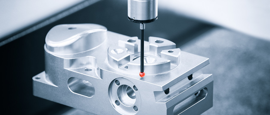
2. Advanced Equipment: Equipped with internationally leading testing instruments to ensure accuracy and reliability of results. Equipped with equipment such as X-RAY, grinding and polishing machines, stereo microscopes, metallographic microscopes, and scanning electron microscopes.
3. Efficient Service: Rapidly respond to customer needs and provide one-stop, high-efficiency inspection services.
4. Authoritative Certification: The laboratory is certified by ISO/IEC 17025, ensuring that test reports have international credibility.

Maxin Testing Laboratory
Learn more about our company

Electronic Manufacturing Information Hub
See more exciting case studies

Video Channel
Watch more exciting videos


 Buildings A1, A3, and A5, Peking University Science and Innovation Park, Songbai Road, Bao'an District, ShenzhenBuilding 3, Xinyao Valley, 415 Changyang Street, Suzhou Industrial Park, Suzhou City1st Floor, Building 4, No. 39 Anzhi Street, Suzhou Industrial Park, Suzhou City


