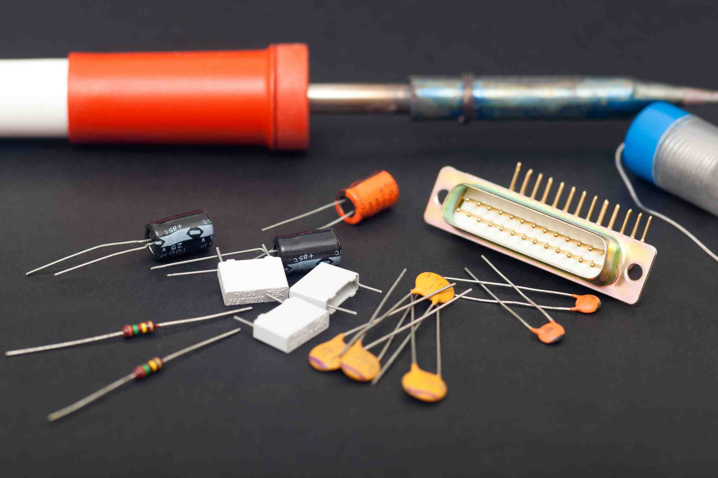


Industries are placing increasing emphasis on issues such as product appearance, with ever-stricter requirements for manufacturing processes. The appearance grading of a product largely reflects its overall quality.

| Overview of Optical Microscopy Project
An optical microscope utilizes the principle of convex lens magnification imaging to enlarge minute objects invisible to the naked eye into sizes that can be discerned by human vision. Its primary function is to increase the visual angle of small nearby objects for the eye (objects with larger visual angles produce larger images on the retina). The wavelength of ordinary light is 400–700 nm, and the optimal resolution of an optical microscope is 0.2 μm, whereas the resolution of the human eye is 0.2 mm. Therefore, the maximum magnification of an optical microscope is generally 1000×. A typical optical microscope is equipped with multiple interchangeable objective lenses, allowing the observer to adjust magnification as required. Since visible light is used as the light source, an optical microscope is highly sensitive and accurate in color recognition. It can observe not only the surface structure of a sample but also tissues beneath the surface within a certain depth.
| Test Objective
Industries are placing increasing emphasis on issues such as product appearance, with ever-stricter requirements for manufacturing processes. The appearance grading of a product largely reflects its overall quality. By using optical magnification devices to inspect product appearance, assembly, and surfaces for defects such as cracks, holes, and poor soldering, it is possible to verify production line processes, assess the quality of printed circuit boards, and detect soldering defects in electronic components. This facilitates monitoring of manufacturing workflows, enables timely corrective actions based on inspection results, and provides guidance for production operations and product quality assurance, thereby ensuring that products meet the shape, fit, and functional requirements under their final operating conditions.
| Testing Standards
IPC-6012 Qualification and Performance Specification for Rigid Printed Boards
IPC-A-610 Acceptability of Electronic Assemblies
IPC-A-600 Acceptability of Printed Boards
| Project Advantages
An optical microscope is characterized by convenient operation, intuitive observation, and high inspection efficiency. It is suitable for surface observation and measurement, enabling the identification and analysis of surface defects of various metals, alloys, and non-metallic products, as well as the inspection of surface phenomena in integrated circuits, printed circuit boards, wires, fibers, and surface coatings. It is also widely applied in the electronics, chemical, and instrumentation industries for observing both opaque and transparent substances.
| Service Products / Fields
According to the functional characteristics of components, acceptance standards generally include three conditions: ideal condition, acceptable condition, and reject condition. It is mainly applied to the inspection and verification of tooling gauges and metal parts, the detection of assembly deviations and soldering abnormalities in electronic products, and the inspection of PCB/PCBA circuitry, solder mask, holes, component alignment, as well as textual and graphical defects.
Testing Procedure:
Confirm sample type → Confirm inspection specification → Place the sample under the optical microscope for observation → Record observed phenomena → Evaluate results.
| MTT Advantages
1. Professional Team: A team of highly experienced testing engineers and technical experts.
2. Advanced Equipment: Equipped with internationally leading testing instruments to ensure accuracy and reliability of results.
3. Efficient Service: Rapidly respond to customer needs and provide one-stop, high-efficiency inspection services.
4. Authoritative Certification: The laboratory is certified by ISO/IEC 17025, ensuring that test reports have international credibility.