


 +86-400-850-4050


Didn't find what you were looking for?
Consult a professional engineer immediately for your service


Atomic Force Microscopy (AFM) operates on the principle of atomic-scale force interactions between a sharp probe tip and the sample surface, which gives the technique its name.
| Project Overview
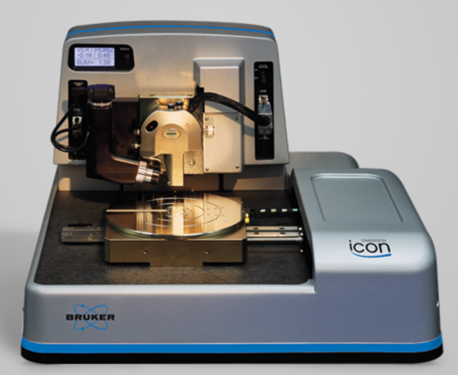
Atomic Force Microscopy (AFM) operates on the principle of atomic-scale force interactions between a sharp probe tip and the sample surface, which gives the technique its name. AFM is suitable for the analysis of various materials and products, such as metallic materials and polymeric compounds. It can be operated under different environments, including ambient atmosphere, vacuum, electrical conditions, and liquid phases, to conduct diverse physical property analyses. Its most distinctive feature is the ability to operate in both air and liquid environments, which makes AFM widely applicable in areas such as biomaterials, crystal growth, and force interaction studies. Depending on the nature of the probe tip and sample material as well as the probe–sample distance, the interaction forces between the tip and the sample may include interatomic repulsive forces, van der Waals attractive forces, elastic forces, adhesion forces, magnetic forces, electrostatic forces, and frictional forces generated during scanning. By controlling and detecting these interaction forces between the probe tip and the sample, AFM can not only characterize surface morphology with high resolution but also analyze surface properties corresponding to different forces. For example, Friction Force Microscopy can be used to study the friction coefficient of materials; Magnetic Force Microscopy can investigate magnetic domain distributions on the sample surface, serving as a powerful tool for analyzing magnetic materials; Electrostatic Force Microscopy can measure surface potential, dielectric constants of thin films, and deposited charges. In addition, AFM can manipulate, modify, and process atoms and molecules, enabling the design and creation of new structures and materials.
| Project Objective
1. Surface Morphology: Direct observation of the surface topography and roughness of samples.
2. Physical Properties: Such as mechanical properties, hardness, and viscoelasticity.
3. Roughness Parameters: Including Ra, Rq, Rz, and others.
4、颗粒度和孔结构:可以分析样品的颗粒度、孔径分布等。
4. Particle Size and Pore Structure: Analysis of particle size, pore size distribution, and related features.
5. Compressive Young’s Modulus: Measurement of the elastic properties of materials.
| Test Standard
GB/T 31227
| Service Products / Fields
AFM is an important nanoscale characterization technique, widely applied in materials science, biology, and related fields.
It is also extensively applied in crystal growth studies and force interaction research.
| Project Advantages
1. Professional Team: Equipped with a number of highly experienced testing engineers and technical experts.
2. Advanced Equipment: Equipped with internationally leading testing instruments to ensure accuracy and reliability of results.
3. Efficient Service: Rapid response to customer needs, capable of testing a wide variety of materials while efficiently and quickly producing authentic and accurate scan images.
4. Authoritative Certification: The laboratory is certified by ISO/IEC 17025, ensuring that test reports have international credibility.
| General Sample Requirements
1. Sample Condition: Samples may be in the form of powders, bulk materials, or thin films.
2. Powder Samples: For routine testing projects, the sample surface irregularity should generally not exceed 5 μm; for special testing projects, the irregularity should generally not exceed 1 μm. A minimum of 20 mg of powder or no less than 1 ml of liquid shall be provided.
3. For powder/liquid samples, preparation conditions shall be clearly indicated, including dispersion medium, ultrasonic treatment time, and preparation concentration.
4. Thin Film or Bulk Sample Size Requirements: Length and width between 0.5–3 cm, thickness between 0.1–1 cm, and surface roughness not exceeding 5 μm. The test surface shall be clearly marked. Bulk samples shall be securely fixed to prevent shaking or friction during transportation, which may affect test results.
5. For materials tested with PFM, KPFM, C-AFM, or PeakForce TUNA, the sample shall be prepared on a conductive substrate, and the substrate size should meet the dimensional requirements of bulk samples. Samples for KPFM, C-AFM, and PeakForce TUNA shall be conductive or at least semiconductive.
6. For PFM and KPFM testing, the sample surface shall be very smooth, with an optimal roughness range of 10–200 nm. Powder samples are difficult to obtain good results from; please ensure risks are acceptable before placing an order.

Maxin Testing Laboratory
Learn more about our company

Electronic Manufacturing Information Hub
See more exciting case studies

Video Channel
Watch more exciting videos


 Buildings A1, A3, and A5, Peking University Science and Innovation Park, Songbai Road, Bao'an District, ShenzhenBuilding 3, Xinyao Valley, 415 Changyang Street, Suzhou Industrial Park, Suzhou City1st Floor, Building 4, No. 39 Anzhi Street, Suzhou Industrial Park, Suzhou City


