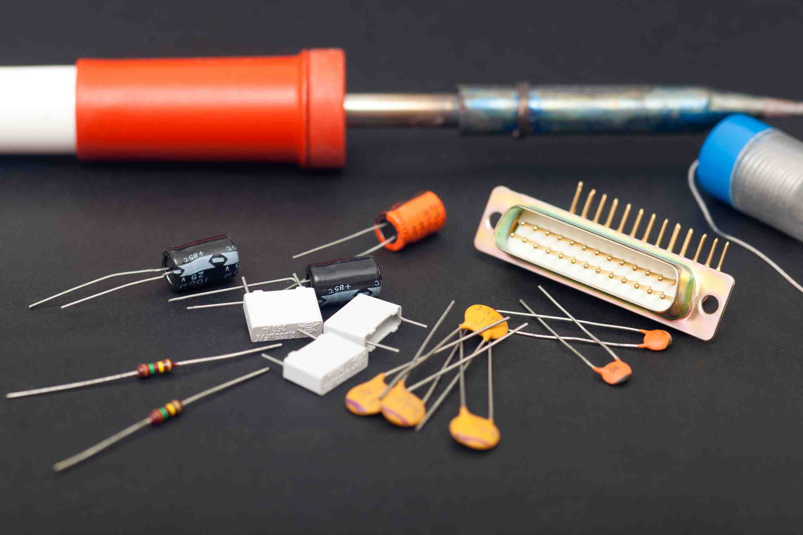


Delayering testing (also referred to as decapsulation or de-packaging testing) is a detection technique that removes the packaging materials of electronic components (such as plastics, ceramics, or metals) by chemical, physical, or mechanical methods to expose internal structures including the chip, bonding wires, and solder joints.

| Project Overview
Delayering testing (also referred to as decapsulation or de-packaging testing) is a detection technique that removes the packaging materials of electronic components (such as plastics, ceramics, or metals) by chemical, physical, or mechanical methods to expose internal structures including the chip, bonding wires, and solder joints. Its core lies in achieving layer-by-layer removal of the package without damaging the internal devices, thereby enabling microscopic observation or analysis (such as electron microscopy or energy spectrum analysis) of internal defects, process quality, or failure mechanisms. Depending on the type of packaging material, delayering methods can be classified as chemical delayering, physical delayering, or mechanical delayering.
| Test Objective
1. Internal Structure Observation: Expose internal components such as chips, bonding wires, and solder joints to examine bonding quality, chip cracks, foreign particle contamination, and other defects.
2. Failure Analysis: Use delayering to locate failure sources (such as chip breakdown, bond detachment, or solder joint cracking) and assist in tracing root causes.
3. Process Verification: Validate the consistency of packaging processes (such as bonding strength) and assess the impact of new materials or new processes on internal structures.
4. Reverse Engineering: In R&D or competitive product analysis, delayering can be used to obtain information on chip design and packaging structure, thereby supporting product optimization.
5. Reliability Assessment: After environmental testing (such as high-temperature exposure), perform delayering to inspect degradation of internal structures, such as corrosion or delamination.
| Testing Standards
GJB 4027B-2021、GJB 548C-2021、MIL-STD-883H.
| Service Products / Fields
Semiconductors and integrated circuits, aerospace and defense, automotive electronics, consumer electronics and communications, research and development.
| Project Advantages
1. Visualization of Internal Defects: Break through the packaging barrier to directly observe microscopic defects of chips and interconnect structures, providing intuitive evidence for failure analysis.
2. High-Precision Operation Assurance: By applying standardized delayering processes (such as controlling chemical etching rates or laser power), avoid damage to internal devices and ensure analytical accuracy.
3. Multi-Dimensional Analysis Compatibility: After delayering, combine techniques such as SEM, energy-dispersive spectroscopy (EDS), and X-ray analysis to conduct comprehensive evaluations of material composition and defect morphology.
4. Full Lifecycle Quality Control: Applicable to R&D validation, production sampling, and failure traceability, covering quality requirements throughout the entire process from design to application.
| MTT Advantages
1. Professional Team: A team of highly experienced testing engineers and technical experts.
2. Advanced Equipment: Equipped with internationally leading testing instruments to ensure accuracy and reliability of results.
3. Efficient Service: Rapidly respond to customer needs and provide one-stop, high-efficiency inspection services.
4. Authoritative Certification: The laboratory is certified by ISO/IEC 17025, ensuring that test reports have international credibility.