


 +86-400-850-4050


Didn't find what you were looking for?
Consult a professional engineer immediately for your service


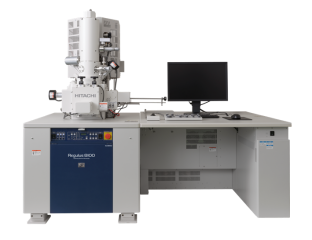
A Scanning Electron Microscope (SEM) scans the surface of a sample with an electron beam and generates images based on signals such as secondary electrons and backscattered electrons. With a resolution reaching the nanometer scale (1–10 nm), it enables intuitive observation of microscopic morphology, compositional distribution, and defect features of the sample.
| Project Overview
A Scanning Electron Microscope (SEM) scans the surface of a sample with an electron beam and generates images based on signals such as secondary electrons and backscattered electrons. With a resolution reaching the nanometer scale (1–10 nm), it enables intuitive observation of microscopic morphology, compositional distribution, and defect features of the sample. Under military standards, SEM inspection must be combined with sample preparation steps (such as decapsulation and sectioning). It is applicable to the microstructural analysis of microelectronic devices, failed components, and discrete devices.
| Test Objective
1. Reliability Evaluation:
Detect cracks at the root of bonding wires (microscopic damage in gold wires with a diameter ≤ 25 μm).
Analyze the microstructure of solder layers (such as SnAgCu alloy) and the distribution of voids.
2. Process Verification: Verify the impact of packaging processes (such as reflow soldering temperature profiles) on the microstructure.
| Testing Standards
GJB 4027B-2021、GJB 128B-2021、GJB 548C-2021
| Service Products / Fields
Manufacturing industry, aerospace and automotive industries, electronics sector, materials and scientific research fields, as well as R&D pilot production testing.
| Project Advantages
1. Nanometer-Scale Defect Identification: Capable of observing interfacial cracks and oxide layer damage at the scale of 10 nm.
2. Three-Dimensional Morphology Reconstruction: Simulate the three-dimensional structure of solder joints through multi-angle SEM imaging to assess stress concentration risks.
3. Correlation with Electrical Performance: For example, correlation analysis between the degree of oxidation at the bonding interface and the contact resistance.
| MTT Advantages
1. Professional Team: A team of highly experienced testing engineers and technical experts.
2. Advanced Equipment: Equipped with internationally leading testing instruments to ensure accuracy and reliability of results.
3. Efficient Service: Rapidly respond to customer needs and provide one-stop, high-efficiency inspection services.
4. Authoritative Certification: The laboratory is certified by ISO/IEC 17025, ensuring that test reports have international credibility.

Maxin Testing Laboratory
Learn more about our company

Electronic Manufacturing Information Hub
See more exciting case studies

Video Channel
Watch more exciting videos


 Buildings A1, A3, and A5, Peking University Science and Innovation Park, Songbai Road, Bao'an District, ShenzhenBuilding 3, Xinyao Valley, 415 Changyang Street, Suzhou Industrial Park, Suzhou City1st Floor, Building 4, No. 39 Anzhi Street, Suzhou Industrial Park, Suzhou City


