+86-400-850-4050


Didn't find what you were looking for?
Consult a professional engineer immediately for your service


By observing material surface morphology with a Scanning Electron Microscope (SEM), convenience is provided for studying the morphological structure of samples, which assists in monitoring product quality and improving processes.
| Project Background
The microscopic geometric morphology of a material’s surface significantly influences many of its technical properties and functional performance. In recent years, with advances in science and technology, increasingly stringent requirements have been placed on the surface precision of various materials.
| Project Overview
Scanning Electron Microscopy (SEM) is currently one of the most commonly used analytical techniques for surface morphology observation. It features high resolution and high magnification; excellent depth of field, broad field of view, and strong three-dimensional imaging; direct observation of subtle structures on irregular sample surfaces; simple specimen preparation; and is equipped with an Energy Dispersive X-ray Spectroscopy (EDS) system, enabling simultaneous morphology observation and micro-area compositional analysis.
By observing material surface morphology with a Scanning Electron Microscope (SEM), convenience is provided for studying the morphological structure of samples, which assists in monitoring product quality and improving processes.
The primary focus of observation is the analysis of material geometric morphology, particle size, particle size distribution, and phase structure.
| Testing Standards
JYT 010-1996 General Principles of Analytical Scanning Electron Microscopy Methods
| Service Products / Fields
Materials, electronics, metallurgy, aerospace, automotive electronics, medicine, machining, semiconductor manufacturing, ceramics, and others.
Testing Procedure:
The sample surface is sputter-coated with platinum, then placed into the SEM sample chamber following standard operating procedures. The specified test locations required by the customer are magnified, observed, and measured.
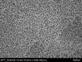
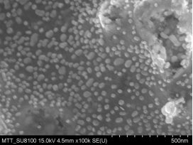
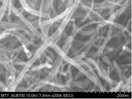
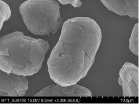
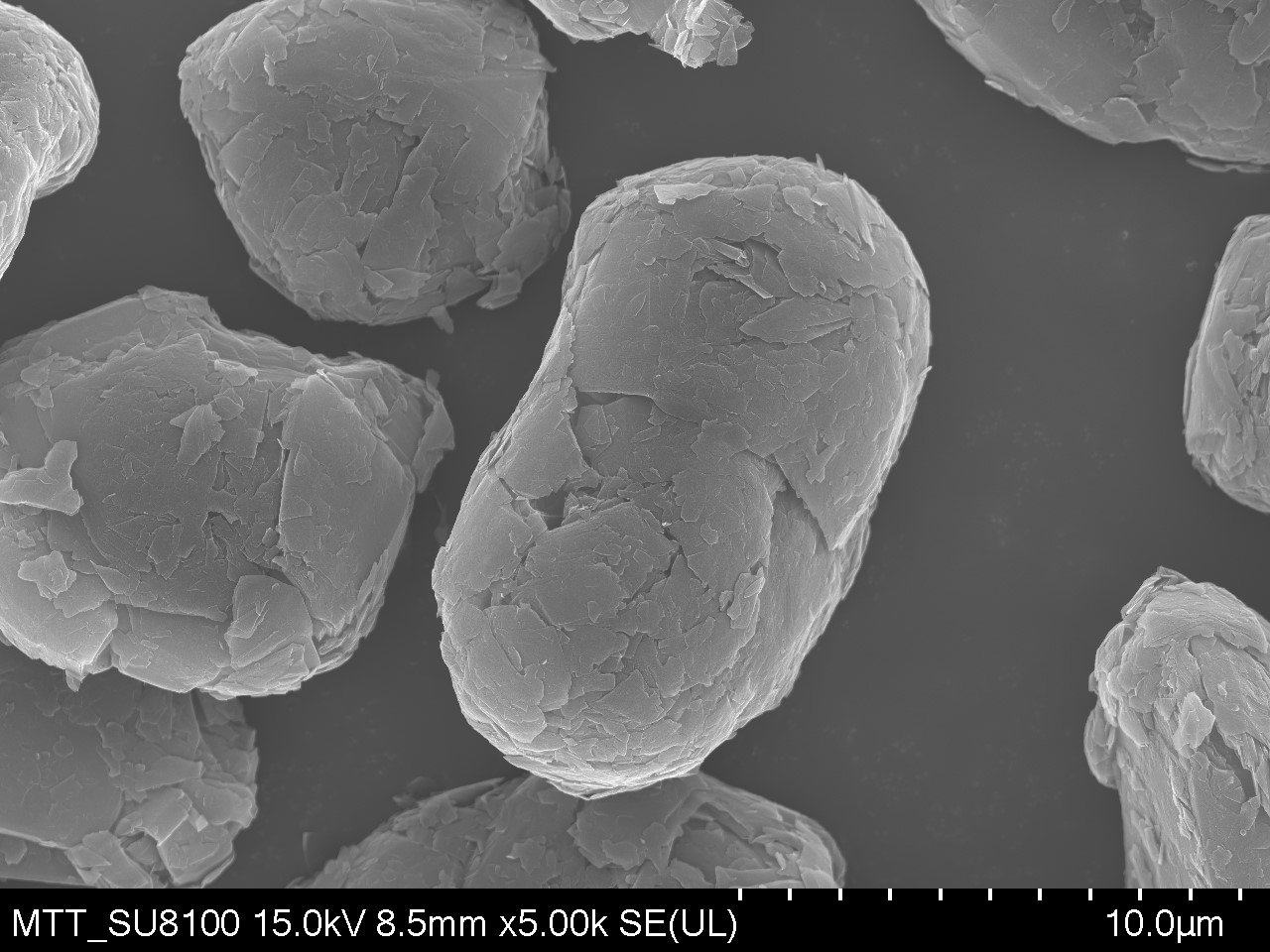
| Typical Images
|
|
|
|
Metallic Nanopores |
Pt Catalyst |
|
|
|
|
Carbon nanotubes |
Graphene |
| MTT Advantages
1. Professional Team: A team of highly experienced testing engineers and technical experts.
2. Advanced Equipment: Equipped with internationally leading testing instruments to ensure accuracy and reliability of results.
3. Efficient Service: Rapidly respond to customer needs and provide one-stop, high-efficiency inspection services.
4. Authoritative Certification: The laboratory is certified by ISO/IEC 17025, ensuring that test reports have international credibility.

Maxin Testing Laboratory
Learn more about our company

Electronic Manufacturing Information Hub
See more exciting case studies

Video Channel
Watch more exciting videos


 Buildings A1, A3, and A5, Peking University Science and Innovation Park, Songbai Road, Bao'an District, ShenzhenBuilding 3, Xinyao Valley, 415 Changyang Street, Suzhou Industrial Park, Suzhou City1st Floor, Building 4, No. 39 Anzhi Street, Suzhou Industrial Park, Suzhou City