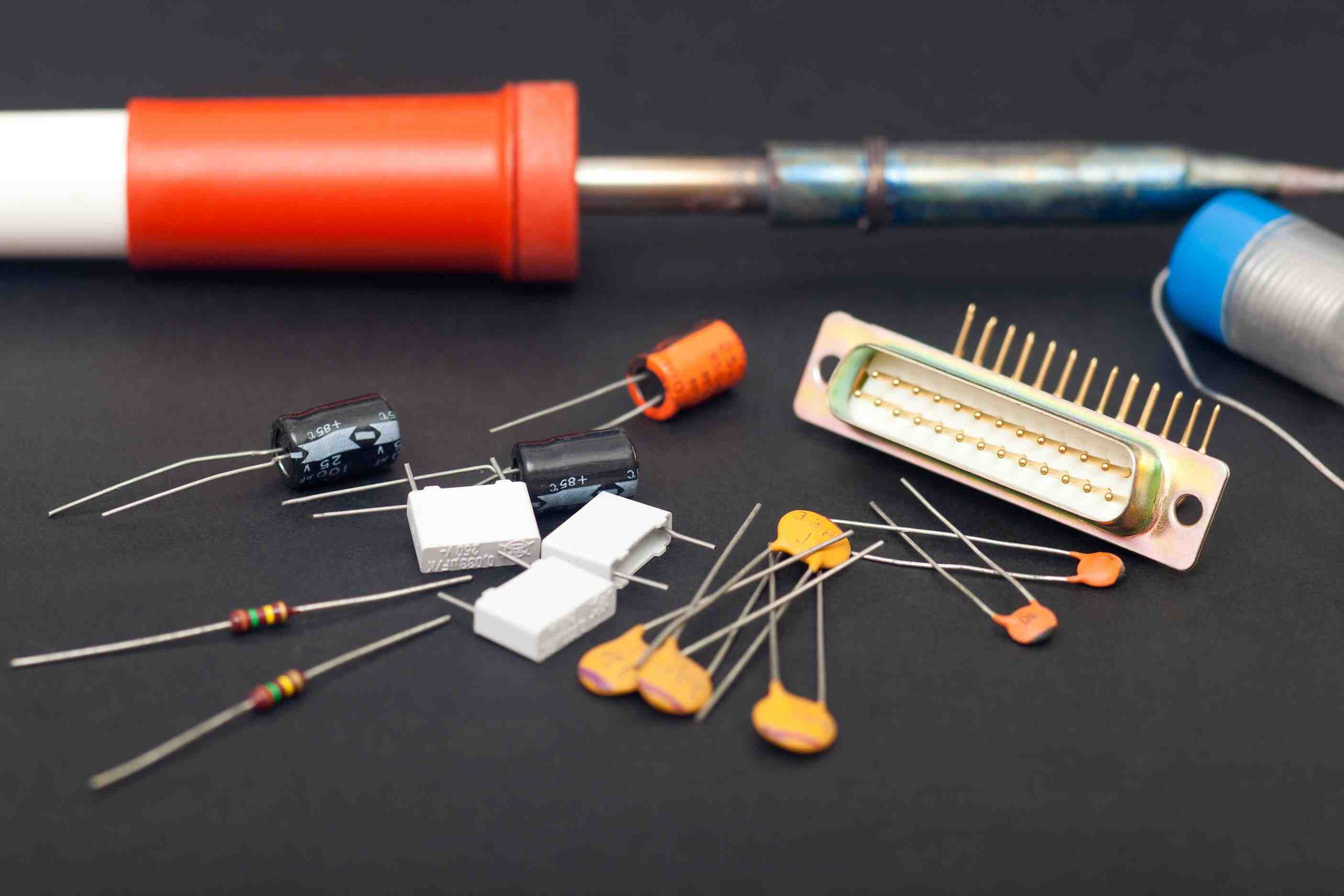
Printed circuit boards and their assemblies (PCB & PCBA) are the core components of electronic products, and their reliability directly determines the overall reliability of electronic products. To ensure and enhance the quality and reliability of electronic products, it is essential to carry out comprehensive physical and chemical analyses of failures, identify the underlying failure mechanisms, and then propose corresponding improvement measures. MTT possesses profound technical expertise in board-level failure analysis, a complete range of analytical methods, a vast database of case studies, and a team of experienced experts, providing you with high-quality and efficient failure analysis services.
The purpose of electronic component failure analysis is to employ a variety of testing and analytical techniques and procedures to identify the failure phenomena of electronic components, determine their failure modes and mechanisms, identify the ultimate root cause of failure, and propose recommendations for improvements in design and manufacturing processes. This helps prevent the recurrence of failures and improves the overall reliability of the components.
The continuous rise in complexity and performance requirements of integrated circuits, combined with potential risks across design, manufacturing, packaging, and application stages, has led to frequent occurrences of critical failure modes such as short circuits, open circuits, leakage, burnout, and parameter drift. These issues not only result in costly device scrapping and system downtime but also often trigger disputes over responsibility among designers, foundries, packaging and testing houses, and end-users, causing significant economic losses and reputational risks.
The performance requirements for polymer materials continue to rise, while differences in understanding of high-demand products and processes between customers and suppliers often lead to frequent failures such as fracture, cracking, corrosion, and discoloration. These failures frequently cause disputes over responsibility and result in significant economic losses.
The increasingly harsh service environments of metal components place higher demands on material performance and structural reliability. However, factors such as design flaws, material defects, manufacturing deviations, or improper use can readily trigger typical failures including fatigue fracture, stress corrosion cracking, hydrogen embrittlement, creep, wear, and overload deformation.
Didn't find what you were looking for?
Consult a professional engineer immediately for your service
Didn't find what you were looking for?
Consult a professional engineer immediately for your service
Meixin Testing leverages its technological edge in constructing massive failure databases, showcasing its capabilities through comprehensive case studies, solutions for complex scenarios, partnerships with leading enterprises, and systematic intellectual property. Drawing on millions of failure analyses, it delivers precise insights into root causes, enabling inspection reports to provide robust support for clients' quality upgrades and achieve zero failures.
Didn't find what you were looking for?
Consult a professional engineer immediately for your service
Stay updated with the latest news from Maxin Testing, including technical developments, exhibitions, and events. We build on a foundation of professional testing to deliver customized solutions for our clients, ensuring quality control from the source. This empowers our clients to stand out in the marketplace and achieve commercial success.
Didn't find what you were looking for?
Consult a professional engineer immediately for your service
Maxin Testing is a nationally accredited commercial third-party laboratory. We specialize in providing testing services, technical consulting services, and solution services to clients across industries including electronics manufacturing, automotive electronics, semiconductors, and aerospace materials.
Maxin Testing operates laboratory facilities in Shenzhen, Suzhou, and Beijing, featuring multidisciplinary testing and analytical laboratories. The company pioneers an industrial hospital service model grounded in materials science engineering and electronic reliability engineering.
Didn't find what you were looking for?
Consult a professional engineer immediately for your service
Professional verification platform, delivering precise data insights to build a solid foundation of trust for investors.
Didn't find what you were looking for?
Consult a professional engineer immediately for your service
Advanced Material Characterization

The advanced material characterization technology utilizes the interaction between electrons, photons, ions, atoms, strong electric fields, thermal energy, etc., and the solid surface to measure the energy spectra, spectra, mass spectra, spatial distributions, or diffraction images of electrons, photons, ions, atoms, and molecules scattered or emitted from the surface, and characterize relevant parameters such as the surface micro-morphology, surface roughness, surface micro-area composition, surface organizational structure, surface phase structure, surface coating structure and composition of materials.

Advanced Material Characterization

| Project Overview


The advanced material characterization technology utilizes the interaction between electrons, photons, ions, atoms, strong electric fields, thermal energy, etc., and the solid surface to measure the energy spectra, spectra, mass spectra, spatial distributions, or diffraction images of electrons, photons, ions, atoms, and molecules scattered or emitted from the surface, and characterize relevant parameters such as the surface micro-morphology, surface roughness, surface micro-area composition, surface organizational structure, surface phase structure, surface coating structure and composition of materials.


| Commonly Used Detection Technologies


Technologies such as X-ray energy spectrum analysis (EDS), Auger electron spectroscopy (AES), X-ray photoelectron energy spectrum analysis (XPS), dynamic secondary ion mass spectrometry analysis (D-SIMS), time-of-flight secondary ion mass spectrometry analysis (TOF-SIMS), focused ion beam analysis (FIB), and ion grinding and polishing (CP).


· X-ray photoelectron energy spectrum analysis (XPS)

X-ray photoelectron energy spectrum can not only determine the constituent elements on the surface but also provide information on the chemical states of each element. It has high energy resolution and a certain spatial resolution (currently on the micrometer scale). It is used to determine the constituent elements on the surface and provide information on the chemical states of each element.


1. Qualitative and quantitative analysis of elements from Li to U

2. Valence state analysis of elements from Li to U

3. Detection limit: 0.1%

4. UPS function (work function, valence band spectrum)

5. In-depth analysis with a maximum depth of 1 μm

6. The minimum analysis area is 30-400 μm, and the depth is 5-10 nm


Application Cases

Analysis of surface elements and valence states of zirconium alloy tubes after high-temperature friction


· Time-of-flight secondary ion mass spectrometry analysis (TOF-SIMS)


Time-of-flight secondary ion mass spectrometry excites the sample surface with primary ions to eject a tiny number of secondary ions. The mass of the ions is determined based on the different times it takes for the secondary ions to reach the detector due to their different masses. It can provide structural information such as elements and molecules of surfaces, thin films, interfaces, and even three-dimensional samples. Its characteristic is that the secondary ions come from a single atomic or molecular layer on the surface (within 1 nm), carrying only the chemical information of the surface. It features a small analysis area, shallow analysis depth, and non-destructive testing of the sample.


1. Qualitative analysis of all elements and isotopes (including H)

2. Qualitative analysis of organic molecular formulas and functional groups

3. Detection limit: ppm

4. The minimum analysis area is 1 μm, and the depth is 1-10 nm

5. The maximum area scan is 300X300μm


| MTT Advantages


1. Professional Team: A team of highly experienced testing engineers and technical experts.


2. Advanced Equipment: Equipped with internationally leading testing instruments to ensure accuracy and reliability of results.


3. Efficient Service: Rapidly respond to customer needs and provide one-stop, high-efficiency inspection services.


4. Authoritative Certification: The laboratory is certified by ISO/IEC 17025, ensuring that test reports have international credibility.

Online Service Enquiries
  • * Name:
  • * Email:
  • * Company:
  • Position:
  • * Tel:
  • City:
  • Consultation Content:
1. When you provide personal information to this website, we shall not disclose (share, sell or transfer) any of your personal information to third parties (including companies or individuals) without your prior consent, unless required by law or government mandate.
2. The information you provide will only be used to help us deliver a better service to you.
Online Customer Service
Business Consultation
Free Consultation
Report Inquiry
Back to Top
Contact Us
  • *Name:
  • *Contact:
  • *Email:
  • *Company/Organization/school:
  • *The location:
  • *Message information: