


 +86-400-850-4050


Didn't find what you were looking for?
Consult a professional engineer immediately for your service


Emission Microscope (EMMI) is a tool used for fault point localization and for detecting bright spots and hotspots. It identifies fault points by measuring photons emitted from the sample when a bias voltage is applied.
| Project Overview
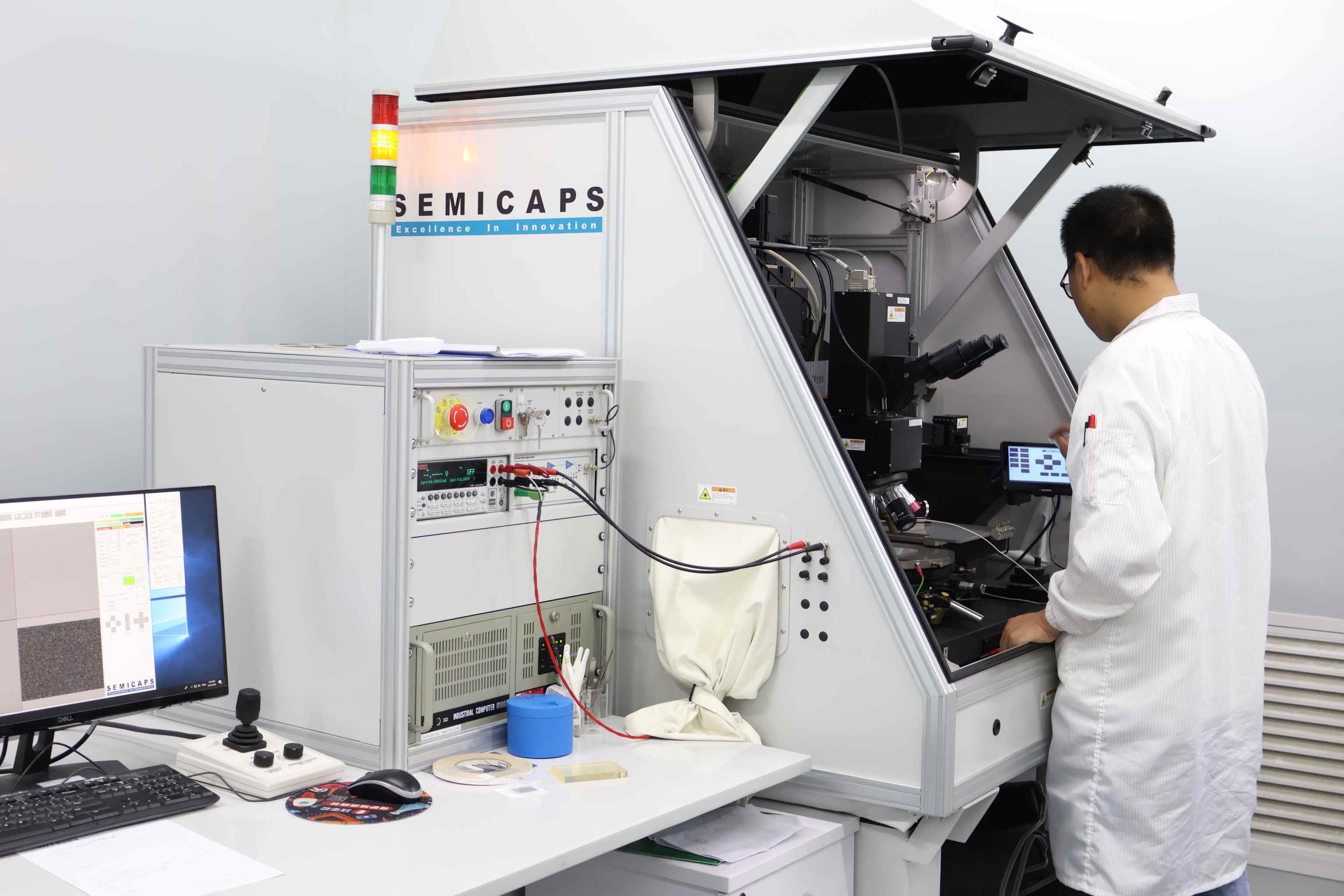
Emission Microscope (EMMI) is a tool used for fault point localization and for detecting bright spots and hotspots. It identifies fault points by measuring photons emitted from the sample when a bias voltage is applied. EMMI can be widely applied to detect leakage currents caused by various component defects, including gate oxide defects, electrostatic discharge (ESD) failures, latch-up effects, leakage, junction leakage, forward bias conditions, and transistors operating in the saturation region.
| Test Objective
Through EMMI localization technology, hotspots or bright spots within samples can be quickly and accurately identified, enabling analysis of the root causes of defect formation. This technology not only improves the efficiency of fault point localization but also provides strong support for subsequent failure analysis, helping to shorten product development cycles and reduce production costs.
| Service Products / Fields
1. Semiconductor Materials: Detection of defects and impurities within the material.
2. Device Defect Detection: Identify and locate fault points within devices.
3. Integrated Circuits: Analyze the causes of failures in integrated circuits.
4. Materials Science: Study the photoelectric properties and failure mechanisms of materials.
5. Nanotechnology: Localize and analyze fault points at the nanoscale.
| Project Advantages
1. High Sensitivity: Capable of capturing extremely weak photon signals to ensure precise fault point localization.
2. Wide Wavelength Detection Range: Covers the near-infrared spectrum, providing broader detection capabilities.
3. Non-Destructive Testing: No destructive treatment of the sample is required, thereby preserving the integrity of the specimen.
4. Broad Application Fields: Suitable for semiconductor materials, device defect detection, integrated circuits, materials science, and nanotechnology.
| MTT Advantages
1. Professional Team: A team of highly experienced testing engineers and technical experts.
2. Advanced Equipment: Equipped with internationally leading testing instruments to ensure accuracy and reliability of results.
3. Efficient Service: Rapidly respond to customer needs and provide one-stop, high-efficiency inspection services.
4. Authoritative Certification: The laboratory is certified by ISO/IEC 17025, ensuring that test reports have international credibility.

Maxin Testing Laboratory
Learn more about our company

Electronic Manufacturing Information Hub
See more exciting case studies

Video Channel
Watch more exciting videos


 Buildings A1, A3, and A5, Peking University Science and Innovation Park, Songbai Road, Bao'an District, ShenzhenBuilding 3, Xinyao Valley, 415 Changyang Street, Suzhou Industrial Park, Suzhou City1st Floor, Building 4, No. 39 Anzhi Street, Suzhou Industrial Park, Suzhou City


