


 +86-400-850-4050


Didn't find what you were looking for?
Consult a professional engineer immediately for your service


Industrial CT technology can accurately and quickly reproduce the three-dimensional structure inside an object, providing quantitative information on the physical and mechanical properties inside the object, such as the location and size of defects, changes in density and level, the shape and precise size of irregular structures, impurities and distribution inside the object, etc.
| What is Nondestructive Testing (NDT)?
Nondestructive testing refers to a method that, without impairing the performance of the object under test or damaging its internal structure, examines and evaluates the internal and surface structures, properties, conditions, and defects of the specimen. It does so by detecting changes in responses such as heat, sound, light, electricity, or magnetism caused by abnormalities or defects in the material’s internal structure. This enables inspection of the type, quantity, shape, location, and size of defects.
| The Significance of Nondestructive Testing
Without damaging the tested object, these measurements help enterprises gain a more comprehensive, direct, and in-depth understanding and evaluation of the properties, conditions, quality, or internal structure of the inspected materials and equipment components. This contributes to monitoring product quality and improving manufacturing processes.
| Service Products / Fields
PCB & PCBA, FPC, electronic and electrical products, electronic components, plastic materials, automotive materials and parts, medical devices, academic/research products, military and defense applications, and more.
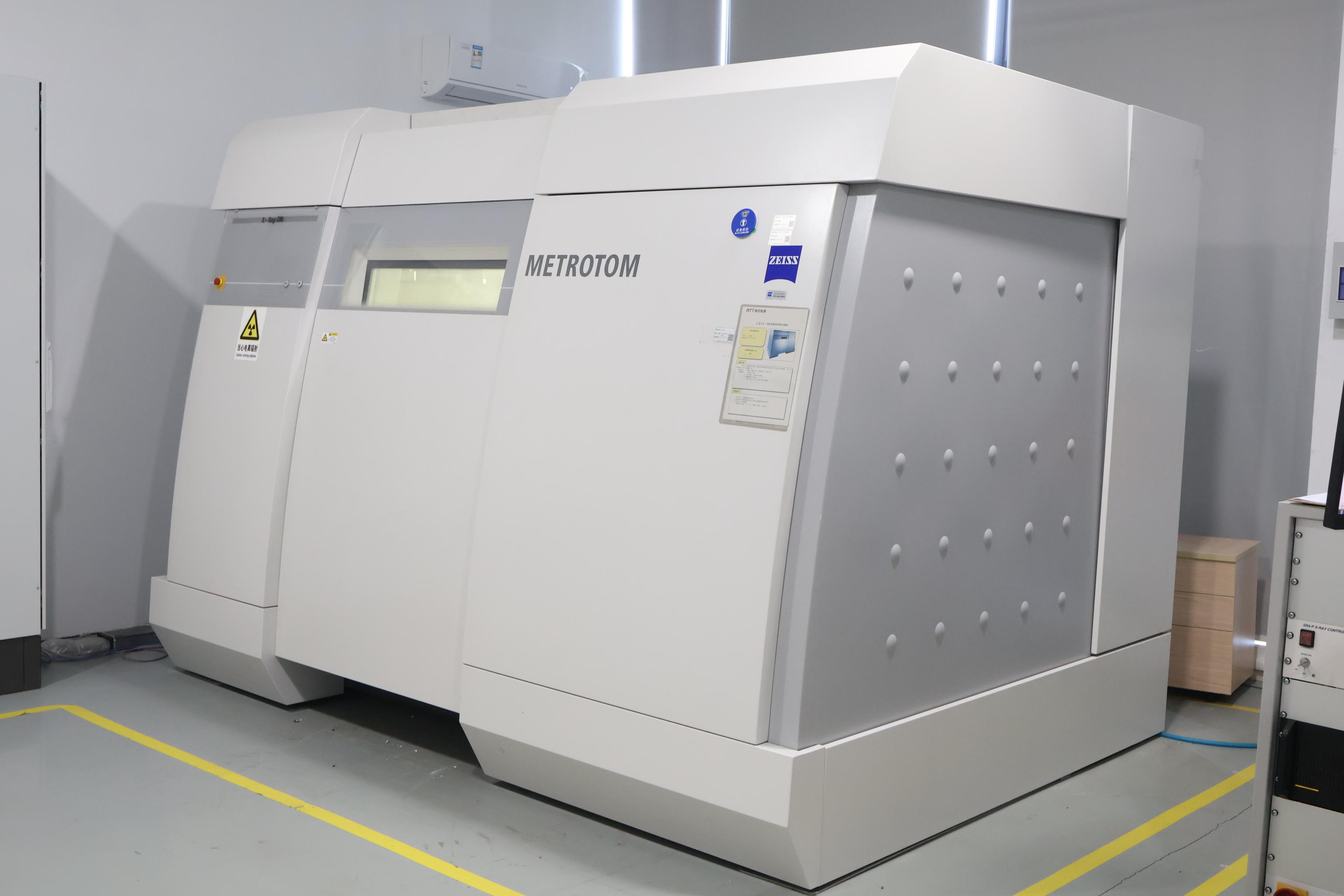
| CT Project Overview
CT technology can accurately and rapidly reconstruct the three-dimensional internal structure of objects. It quantitatively provides physical and mechanical characteristics of the internal structure, such as the location and size of defects, density variations and levels, shapes and precise dimensions of irregular structures, as well as internal impurities and their distribution.
| Project Objective
1. Rapidly, accurately, and intuitively identify internal defects of products (including defect types, locations, and dimensions), such
2. Through CT scanning, the internal structure of the product can be directly observed, enabling measurement of structural dimensions without damaging the sample. Its structural dimensions can thus be determined.
3. CT scanning allows the scan results to be optimally matched with CAD models, using intuitive color deviation maps. These highlight, quickly and vividly, the differences between the target structure and the CAD data.
4. Through CT scanning, the scan results can be exported as point cloud data and quickly output in STL file format for CAD applications.
| Testing Standards
VW50093, PV6093, and others.
| Service Products / Fields
Automotive materials and components, metallic materials, plastic materials, molds, rail transit, electronic and electrical products, medical devices, aerospace, research institutes, and defense industry.
| Testing Procedure
Confirm sample type/material → place into measuring device → rapid scanning → overall imaging and arbitrary sectional views → defect analysis.
| Typical Images
|
|
|
|
Inner layer defects of PCB |
Internal defects of ceramic capacitors |
|
|
|
|
Inspection of welding quality |
BGA solder ball cold solder joint |
| MTT Advantages
1. Professional Team: A team of highly experienced testing engineers and technical experts.
2. Advanced Equipment: Equipped with internationally leading testing instruments to ensure accuracy and reliability of results.
3. Efficient Service: Rapidly respond to customer needs and provide one-stop, high-efficiency inspection services.
4. Authoritative Certification: The laboratory is certified by ISO/IEC 17025, ensuring that test reports have international credibility.

Maxin Testing Laboratory
Learn more about our company

Electronic Manufacturing Information Hub
See more exciting case studies

Video Channel
Watch more exciting videos


 Buildings A1, A3, and A5, Peking University Science and Innovation Park, Songbai Road, Bao'an District, ShenzhenBuilding 3, Xinyao Valley, 415 Changyang Street, Suzhou Industrial Park, Suzhou City1st Floor, Building 4, No. 39 Anzhi Street, Suzhou Industrial Park, Suzhou City


