


 +86-400-850-4050


Didn't find what you were looking for?
Consult a professional engineer immediately for your service


Determine whether the PCB can withstand the thermal stress effects that may be exposed to extremely hot conditions during assembly, rework or repair.
| Project Background
Determine whether the PCB can withstand the thermal stress effects that may be exposed to extremely hot conditions during assembly, rework or repair.
| Project Overview
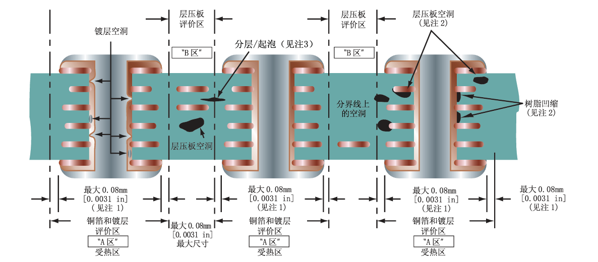
After baking the PCB or components (usually at 120~150 degrees Celsius for at least 6 hours) to remove moisture, process them multiple times in overheated solder (usually at 288 degrees Celsius for 10 seconds). Evaluate through visual inspection (for delamination, blistering, white spots, etc.) or Cross-Section (substrate delamination, cracks, blistering, warping, etc.).
| Test Objective
1. Determine whether the PCB material and process capabilities meet the thermal shock resistance requirements of the product
2. Simulate the usage environment and expose potential risks such as delamination in production in advance
| Testing Standards
IPC-TM 650 2.6.1 Thermal Stress, Laminates
GJB 362 General Specification for Rigid Printed Boards
QJ 832 Test Methods for Multilayer Printed Circuit Boards for Aerospace Use.
| Service Products / Fields
Related products: PCB/FPC
Related fields: Consumer electronics, automotive electronics, aerospace electronic products
| MTT Advantages
1. Professional Team: A team of highly experienced testing engineers and technical experts.
2. Advanced Equipment: Equipped with internationally leading testing instruments to ensure accuracy and reliability of results.
3. Efficient Service: Rapidly respond to customer needs and provide one-stop, high-efficiency inspection services.
4. Authoritative Certification: The laboratory is certified by ISO/IEC 17025, ensuring that test reports have international credibility.

Maxin Testing Laboratory
Learn more about our company

Electronic Manufacturing Information Hub
See more exciting case studies

Video Channel
Watch more exciting videos


 Buildings A1, A3, and A5, Peking University Science and Innovation Park, Songbai Road, Bao'an District, ShenzhenBuilding 3, Xinyao Valley, 415 Changyang Street, Suzhou Industrial Park, Suzhou City1st Floor, Building 4, No. 39 Anzhi Street, Suzhou Industrial Park, Suzhou City


