


 +86-400-850-4050


Didn't find what you were looking for?
Consult a professional engineer immediately for your service


Focused Ion Beam (FIB) non-site-specific cutting is an advanced micro-nano processing technology. It utilizes a focused ion beam to cut materials without the need to predetermine an exact cutting point.
| Project Overview
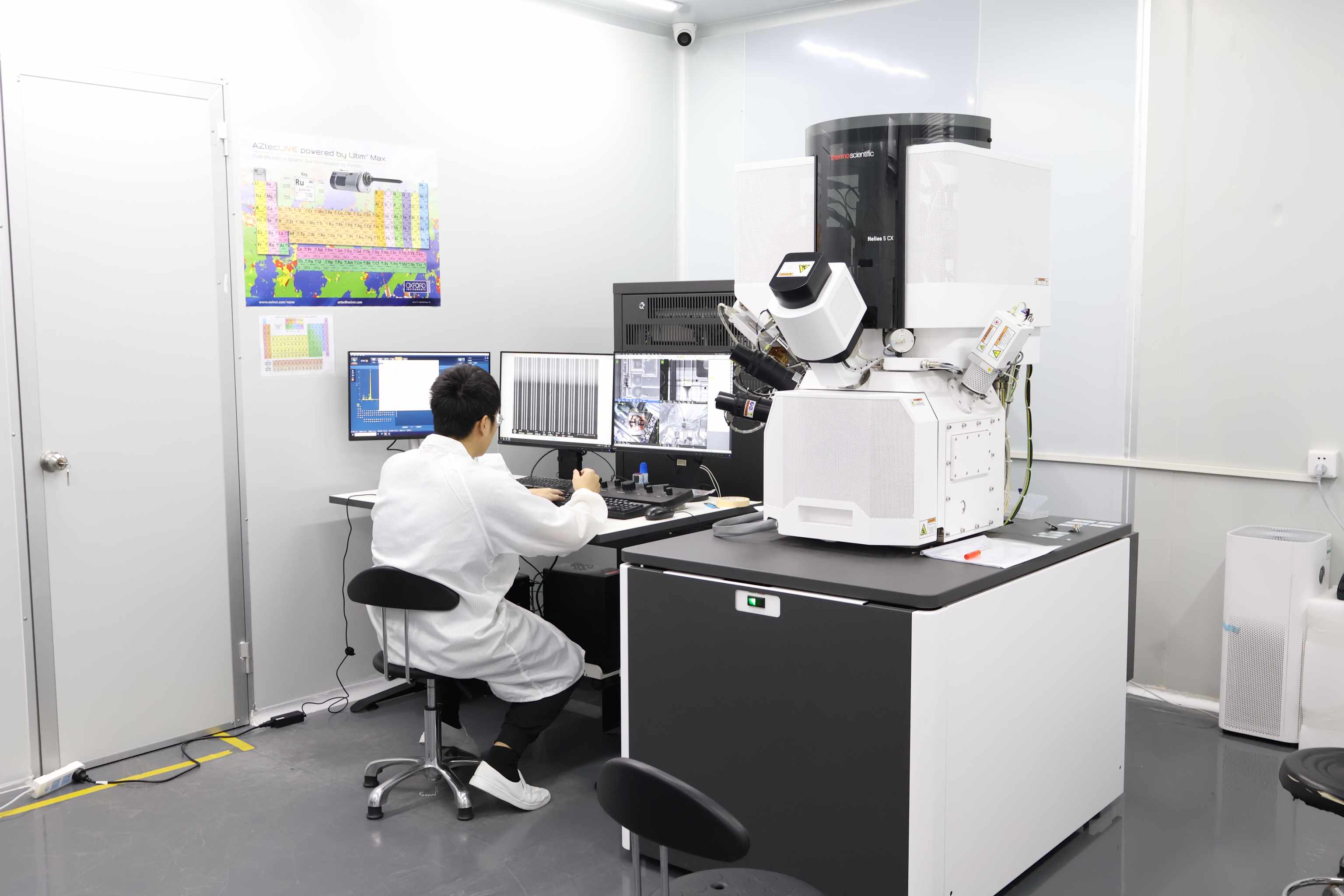
Focused Ion Beam (FIB) non-site-specific cutting is an advanced micro-nano processing technology. It utilizes a focused ion beam to cut materials without the need to predetermine an exact cutting point. The FIB system generates a high-energy ion beam, and by adjusting the beam parameters, the depth and precision of the cut can be controlled. This technology has wide applications in fields such as semiconductors and materials science. It enables rapid cutting of samples to observe internal structures and can also be used to fabricate micro- and nano-structures of specific shapes. The flexibility of non-site-specific cutting allows it to adapt to different experimental needs, providing a powerful tool for research and development.
| Test Objective
1. To quickly analyze the internal structure of samples, there is no need to predefine specific cutting locations; cutting regions can be flexibly selected according to actual observation requirements.
2. In fields such as semiconductors, it helps researchers gain a better understanding of the microscopic properties and performance of materials, providing a basis for the development and improvement of new materials.
3. Assist in failure analysis by performing non-site-specific cutting on problematic samples to locate fault points and causes, thereby supporting corrective measures and repairs.
| Testing Standards
JY/T 0583-2020 General analytical rules for the focused ion beam system.
| Service Products / Fields
Integrated circuit chips, semiconductor devices, printed circuit boards, electronic connectors, optical lenses, nanomaterials, composite materials, and medical devices.
| Project Advantages
1. High precision and high resolution
2. Flexible processing capability
3. Minimal sample damage
4. Can be combined with other technologies
5. High processing efficiency.
| MTT Advantages
1. Professional Team: A team of highly experienced testing engineers and technical experts.
2. Advanced Equipment: Equipped with internationally leading testing instruments to ensure accuracy and reliability of results.
3. Efficient Service: Rapidly respond to customer needs and provide one-stop, high-efficiency inspection services.
4. Authoritative Certification: The laboratory is certified by ISO/IEC 17025, ensuring that test reports have international credibility.

Maxin Testing Laboratory
Learn more about our company

Electronic Manufacturing Information Hub
See more exciting case studies

Video Channel
Watch more exciting videos


 Buildings A1, A3, and A5, Peking University Science and Innovation Park, Songbai Road, Bao'an District, ShenzhenBuilding 3, Xinyao Valley, 415 Changyang Street, Suzhou Industrial Park, Suzhou City1st Floor, Building 4, No. 39 Anzhi Street, Suzhou Industrial Park, Suzhou City


