+86-400-850-4050


Didn't find what you were looking for?
Consult a professional engineer immediately for your service


A sound product PCBA board (bump welding process) burned in use, the original use of A flux when the loss of efficiency, slightly reduced after cleaning, after the replacement of B flux after the non-performing rate zero. This article will find the cause of its failure through a series of professional detection and analysis methods.
1. Appearance analysis
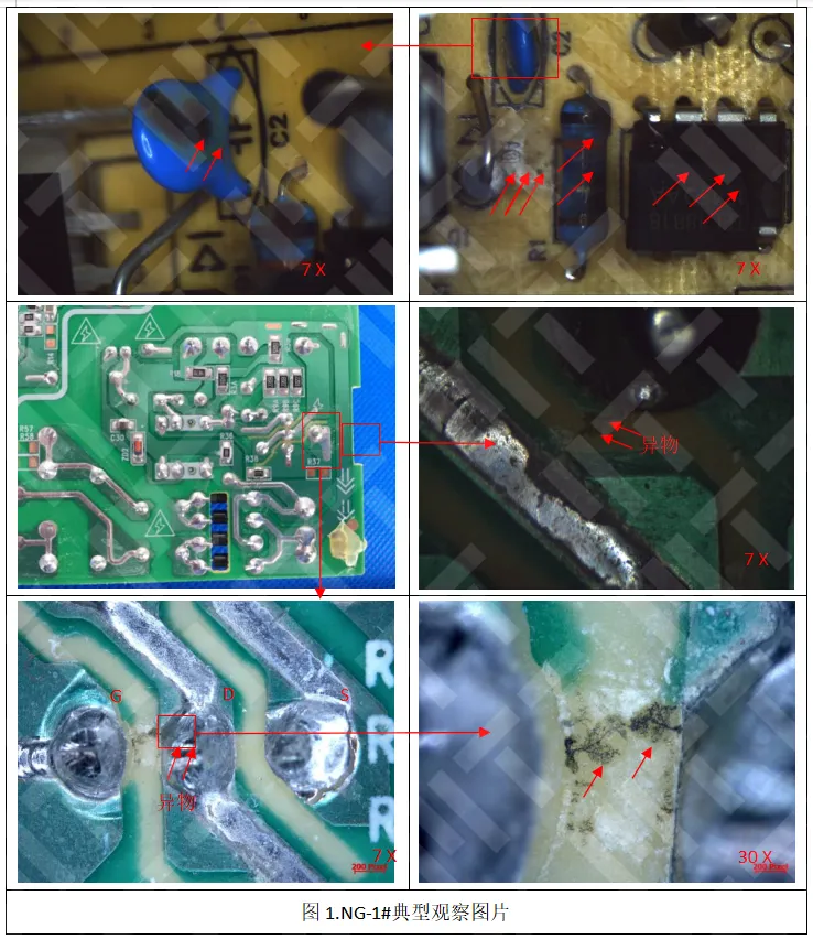
It can be seen from the appearance of the appearance that the NG-0# board burns the most serious, among which the resistance R1 is charred and cracked, the PWM control chip U1 burns and cracks, the diode D1 and the PCB surface of the resistor R1 and MOSFET Q1 have charred traces, and the capacitance C2 surface is slightly charred traces; the NG-1# board burns are consistent with the NG-0# phenomenon, and the NG-2# board is observed to crack the NG-2# plate.
2. Electrical Performance Inspection and Analysis
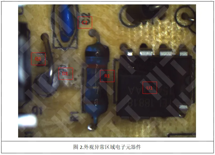
The electronic components with abnormal appearance on the PCBA sample in NG-0# are: MOSFET Q1, diode D1, capacitance C2, resistance R1 and PWM control chip U1 (ITP-LD7535-DIP8).
A. Electrical performance testing
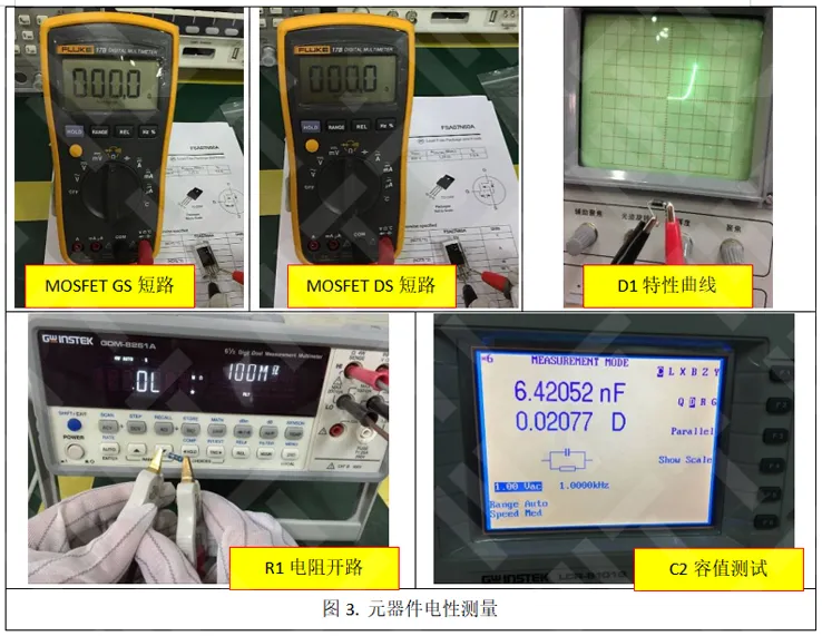
The PWM control chip U1 has been cracked, and the electrical performance test of the remaining related electronic components mentioned above has shown that the short circuit between the MOSFET Q1 pins; the electrical performance of the diode D1 and the capacitor C2 has not been greatly affected; the resistance R1 is open-circuit.
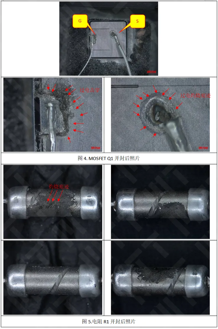
B. Open the inspection
Open the MOSFET Q1, resistor R1 and PWM control chip U1. The opening results show that the insulation near the MOSFET Q1 G electrode has been seriously damaged, which is a typical superimperial breakdown phenomenon, and there are also traces of discharge burning near the S electrode; the conductive film layer on the carbon film resistance R1 has a large area shedding, and there are burn marks on the surface, and corresponds to the crack position observed in the appearance inspection; the PWM control chip U1 has been burned internally, and the burning phenomenon is most obvious in PIN4. Combined with the electrical performance test and the opening test results, it can be initially determined that the device damage is caused by overcurrent and overvoltage.
C. Circuit analysis
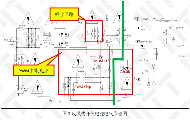
The problem focuses on the reactionary switching power supply circuit shown in the figure, and the circuit design directly related to the appearance of the abnormality mainly includes: absorption circuit and PWM control circuit.
The main role of the absorption circuit in the circuit is to absorb the spike counter voltage and current caused by the MOSFET in the high frequency operating state, and if the peak voltage and current cannot be effectively absorbed, it will affect the reliability of the circuit. The absorption circuit inspection shows that the absorption circuit (including 220K resistor, capacitance C2, diode D1) has normal electrical performance, and the peak voltage absorption function has not failed. This indicates that the absorption circuit is not affected and should work normally.
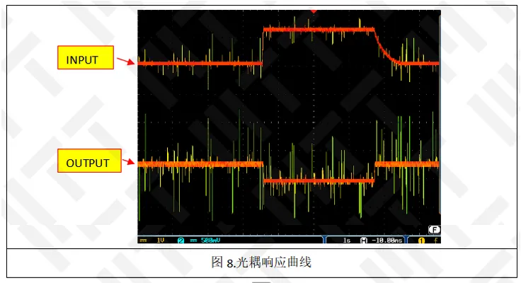
Device damage occurs in the control circuit part, and the direct cause of device damage has been initially analyzed above. Optical coupling is the only device directly connected to the primary circuit (left of the green line) and the secondary circuit (right side of the green line), the photocouple is tested to determine whether the overcurrent and overvoltage are derived from the secondary circuit, the results show that the photocoupled work responds normally (Figure 8), and the secondary circuit has little possibility of overcurrent and overvoltage, which can exclude the influence of the secondary circuit.
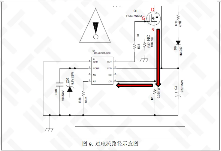
In summary, the circuit analysis range can be reduced to the part shown in Figure 8. This part of the circuit works in the high-voltage state only MOSFET Q1. Resistance R1 (0.36Ω/1W) in the circuit to play a feedback and limit the effect, the resistance due to overcurrent damage, the basic can be determined that the circuit in which the circuit has a large current through, combined with the opening inspection of PIN4 damage is the most obvious phenomenon, can be concluded: overcurrent is due to MOSFET Q1 was broken.
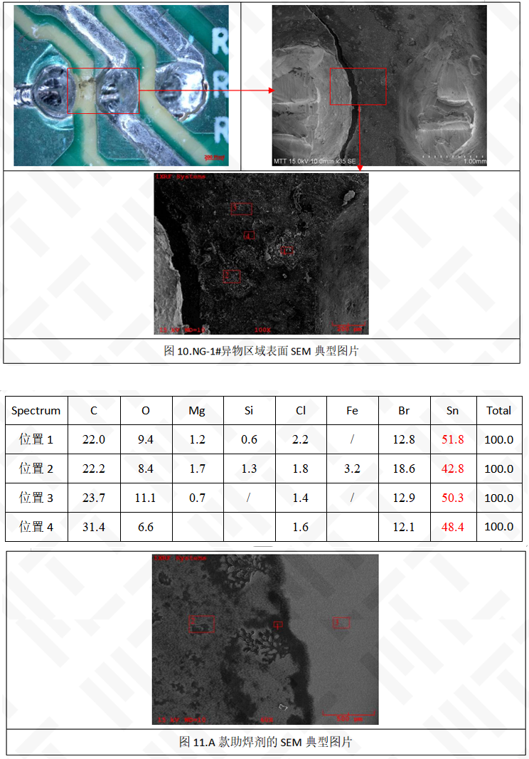
3. SEM+EDS analysis
Compound analysis of foreign body components between G and D pins on the MOSFET Q1 soldered surface PCB on the failed PCB, the results are as follows:
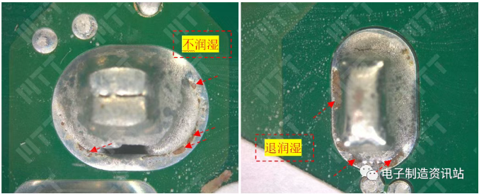
NG-1#: It can be seen from EDS composition analysis that the main components of the foreign body are C, O, Mg, Si, Cl, Br, Sn elements, through amplification observation and confirmation, the main components of the foreign body should be tin slag, and the Sn content between the pins of the PCB board welding surface in MOSFET Q1 is very high, and the position between the pins of the MOS FET in MOSFET Q1 is significantly reduced.
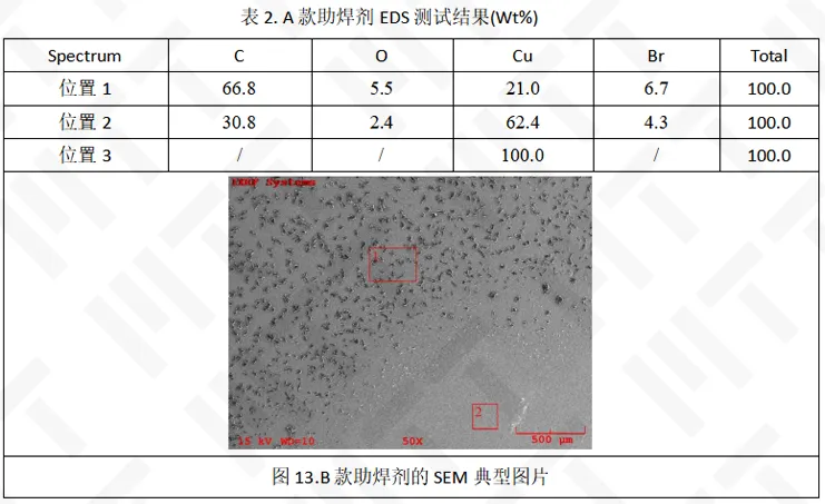
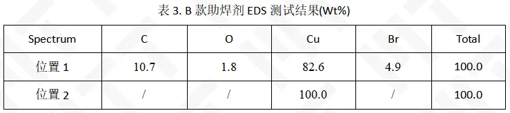
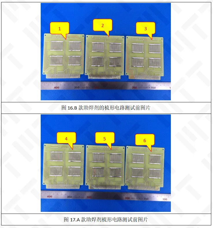
对A款和B款助焊剂的成分进行成分分析发现:A款助焊剂在铜板上的残留较多,B款助焊剂在铜板上的残留很少,两款助焊剂的主要成分都是C、O、Br。
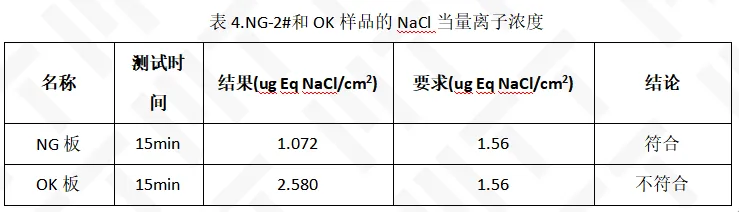
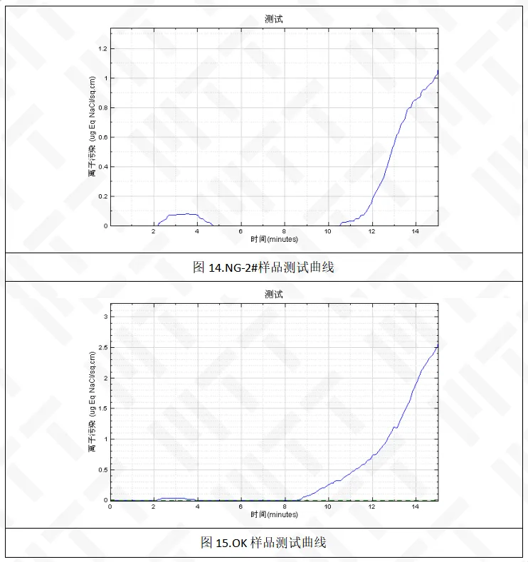
4. Ion Concentration Test Analysis
NG board and OKPCBA board according to IPC-TM-650. 2.3.25C Solvent extraction resistivity (ROSE) NaCl equivalent measurement, the results show: failure plate (NG-2#) surface ion concentration of 1.072μg NaCl/cm2, in line with the standard (≤1.56); normal plate (OK) ion concentration of 2.580μg, exceeded but not burned. Indicates that surface ions are not the main cause of PCBA burning.
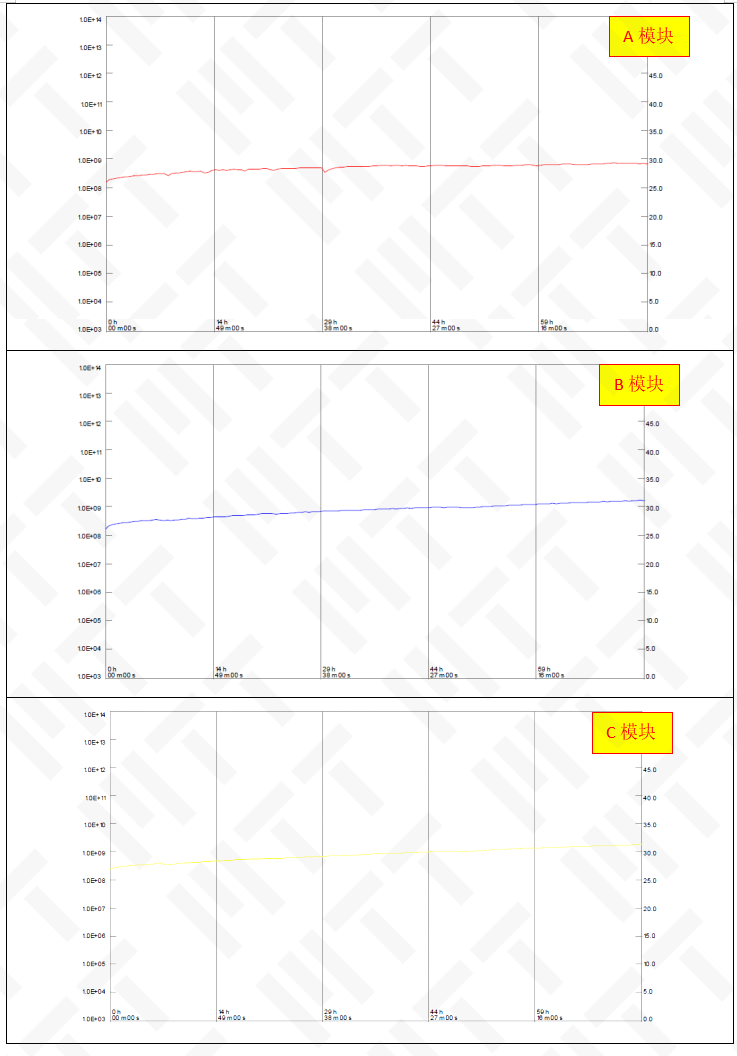
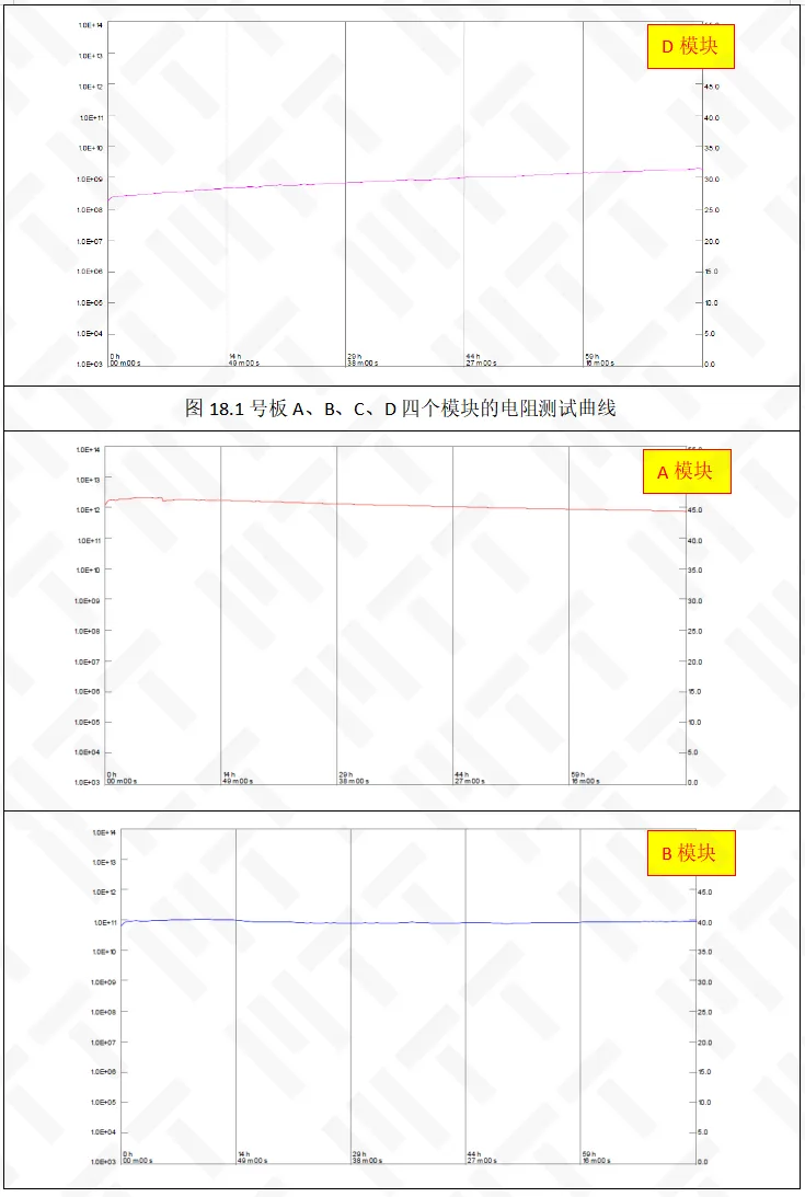
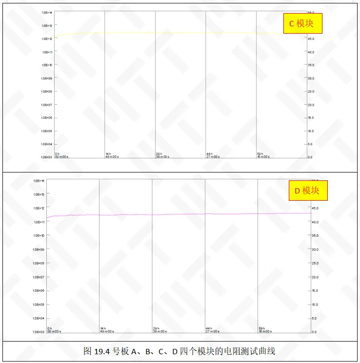
5. Surface Insulation Resistance Testing of Fluxes
For the surface insulation resistance of A and B flux, the surface insulation resistance of the A flux is about between 1011 and 1012 ohms, and the surface insulation resistance of the B flux is probably between 108 and 109 ohms, which meets the standard requirements of more than 108, which shows that the ion residue of the flux is not the cause of PCBA burning.
The direct cause of the PCBA burn is the residual tinlag between the pins of the MOSFET Q1 welding surface, coupled with the flux residue, resulting in a decrease in the insulation resistance of the PCB. Combined with the process to improve feedback, the replacement of flux after the bad rate dropped significantly, indicating that the root cause of the plate burn should be the flux and PCB board compatibility problems.
6. Summary
The direct cause of PCBA burn is that there is a large amount of tin between the MOSFET pins after wave peak welding, and the ion residue of the flux itself, which causes the pressure resistance of the PCB insulation to decrease; the fundamental reason is that there is compatibility between the flux and the PCB board.


Maxin Testing Laboratory
Learn more about our company

Electronic Manufacturing Information Hub
See more exciting case studies

Video Channel
Watch more exciting videos


 Buildings A1, A3, and A5, Peking University Science and Innovation Park, Songbai Road, Bao'an District, ShenzhenBuilding 3, Xinyao Valley, 415 Changyang Street, Suzhou Industrial Park, Suzhou City1st Floor, Building 4, No. 39 Anzhi Street, Suzhou Industrial Park, Suzhou City