+86-400-850-4050


Didn't find what you were looking for?
Consult a professional engineer immediately for your service


OSP surface treatment offers advantages such as simple process control, low cost, and a smooth surface, making it increasingly prevalent in PCB manufacturing. However, during actual production, issues like process defects, improper product storage, or misuse can easily lead to problems on OSP boards, including surface discoloration, uneven coating thickness, poor solderability on pads, cold solder joints, and insufficient solder coverage.
After passing through two wave soldering temperatures, an OSP pad exhibited severe solderability issues. Reducing the wave soldering temperature resolved the solderability problem. This article analyzes the failure causes and mechanisms of poor solderability on OSP pads and proposes improvement suggestions.
1. Visual Inspection
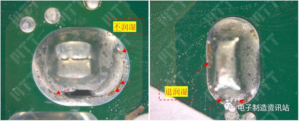
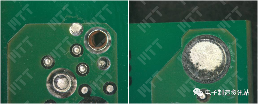
Most solder joints on the NG PCBA exhibited noticeable solder wetting defects on the pad ring surfaces, showing characteristics of de-wetting and non-wetting. Non-wetted areas retained the OSP coating color, suggesting the OSP layer may not have been fully removed.
Figure 1. Photograph of visual inspection showing defective solder joints on NG PCBA after wave soldering
2. Surface Analysis
The surface at the poorly wetted location is smooth with no visible solder residue. Chemical analysis revealed no significant abnormal elements present at the affected area. The Cl element is presumed to originate from residual OSP coating components, which will be further confirmed through additional analytical methods.
Figure 2. Morphological Observation and Composition Analysis of Poorly Wetted Solder Joints on NG PCBA
3. Cross-Section Analysis
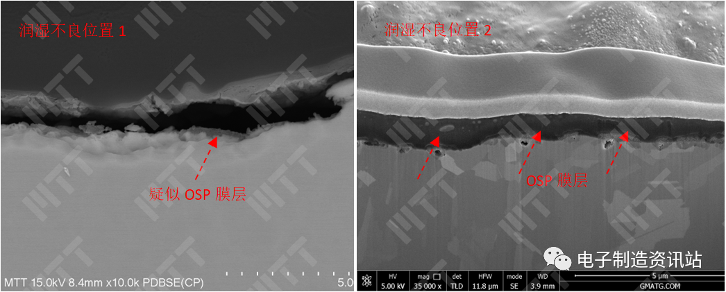
Poorly wetted location 1 shows no obvious solder residue. Upon magnification, localized OSP film residue is suspected.
Poorly wetted location 2 reveals distinct OSP film residue after FIB cutting.
Figure 3. Cross-section observation photos of NG PCBA wave solder joint wettability failure locations after FIB cutting
4. OSP Film Layer Composition Analysis
To characterize the thermal decomposition extent of the OSP organic film and compare whether the OSP film composition differs between the NG batch PCB bare board (designated as Sample A) and the reference PCB bare board (designated as Sample B), the OSP film composition was analyzed for the NG batch PCB bare board, the reference PCB bare board, and the NG batch PCB bare board subjected to secondary reflow (designated as Sample C). The results are as follows.
4.1 FT-IR Analysis
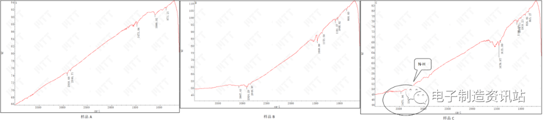
As shown in Figure 4, the infrared spectrum analysis results indicate:
① The infrared spectral information of Sample A's OSP film is weak compared to that of Sample B's OSP film, suggesting Sample A's OSP film may have a thinner layer;
② A new N-H functional group appears in the infrared spectrum of Sample C's OSP film, indicating that the OSP film may have undergone structural changes after secondary reflow.
Figure 4. Infrared Spectrum of OSP Coating Layer
4.2 XPS Analysis
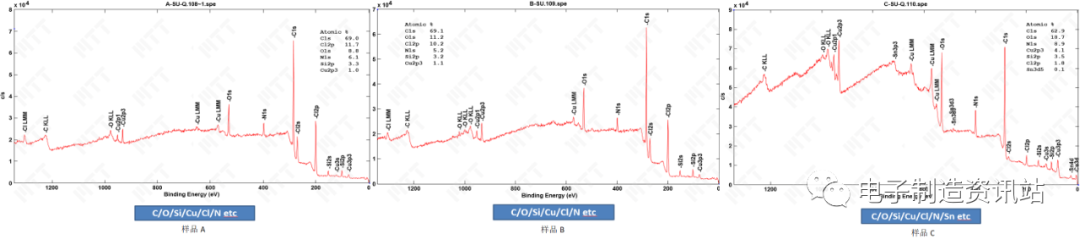
XPS analysis results indicate:
① The OSP coating surfaces of all three samples primarily exhibit elements including C/O/N/Cl/Cu/Si. Sample C also shows trace amounts of Sn;
② The Si on all three surfaces was primarily identified as organosilicon, N as organic nitrogen, and Cl in chemical states including organic chlorine and copper chloride. The compositions of samples A and B were relatively similar: organic compounds exhibited aromatic ring structures (π-π), and copper was mainly present as copper(I) chloride (CuCl). However, no distinct aromatic ring structures were detected on sample C's surface. Instead, ester-type organic compounds were prominent, with copper primarily present as a mixture of copper hydroxide [Cu(OH)₂] and copper(I) chloride (CuCl).
③ The Sn detected on sample C's surface was primarily tin oxide.
Figure 5. XPS Analysis Spectrum
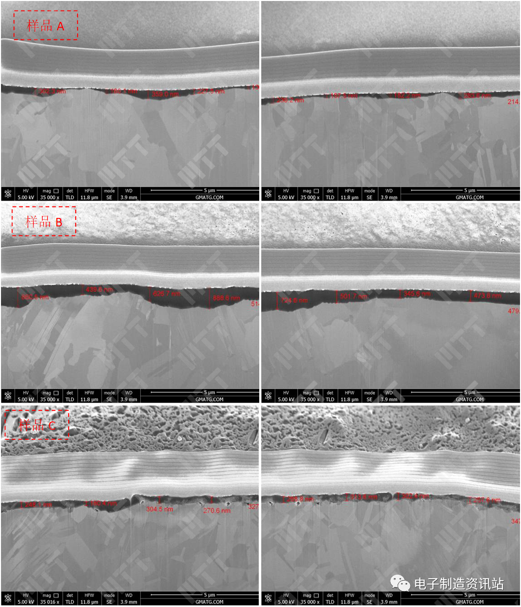
5. OSP Film Thickness Testing
The OSP film layers of Samples A, B, and C were observed and measured for thickness, with the following results:
① The OSP film morphologies of Samples A and B showed no significant differences, but their thicknesses differed markedly;
② The morphology of the OSP coatings on Sample A and Sample C showed distinct differences. Sample C exhibited a dispersed distribution of granular substances within its coating, whereas no such phenomenon was observed in Sample A. The thicknesses of the coatings on Samples A and C were significantly smaller than that of Sample B.
Figure 6. Observation of OSP Film Layer and Film Thickness Measurement Results After FIB Cutting
6. Solderability Verification
To confirm that the PCB blanks from the secondary reflow NG batch indeed exhibited solderability defects and that solderability normalized after reducing the furnace temperature, solderability verification was conducted on both the PCB blanks from the secondary reflow NG batch and the PCB blanks from the secondary reflow NG batch after the furnace temperature reduction.
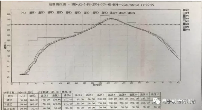
(Note: The reflow profile after lowering the oven temperature meets the lead-free reflow temperature requirements specified in the IPC 7530A-2017 Group Soldering Process Temperature Profile Guide (Reflow and Wave Soldering).)
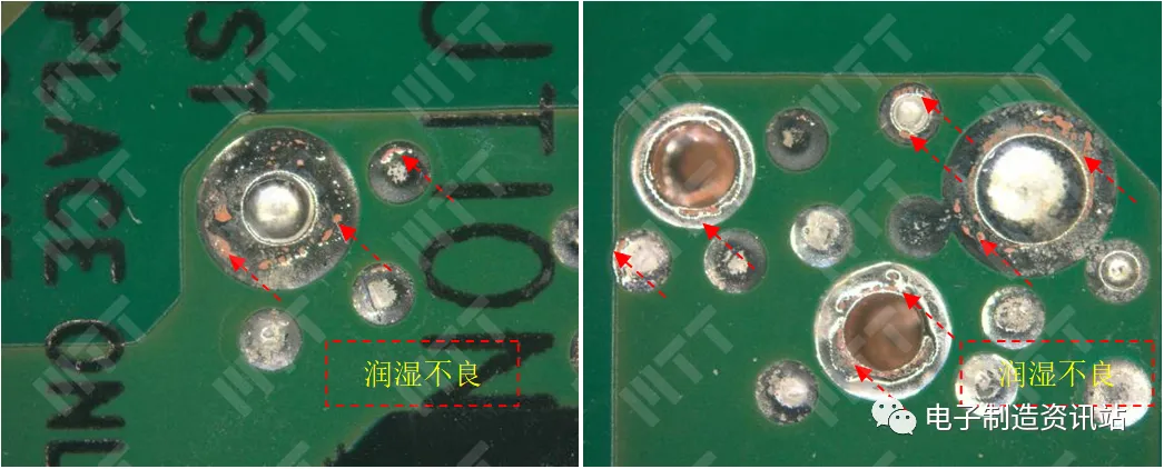
After tin immersion, most through-hole plating rings on the secondary reflow NG batch PCB blanks exhibited significant wetting defects. However, after tin immersion of the secondary reflow NG batch PCB blanks following the reduced oven temperature, the through-hole plating rings demonstrated complete wetting.
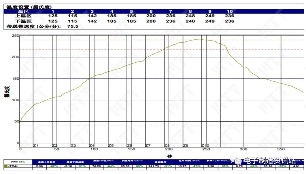
These results indicate: When the oven temperature is adjusted to the range specified for lead-free reflow temperatures in the IPC 7530A-2017 Group Soldering Process Temperature Profile Guide (Reflow and Wave Soldering), solder application on NG batch PCB blanks is normal, meaning the solderability of NG batch PCB blanks meets standard requirements. The peak temperature of the initial oven temperature profile reached a maximum of 245.3°C, which is at the upper limit of the lead-free reflow temperature requirements specified in the IPC 7530A-2017 Group Soldering Process Temperature Profile Guide (Reflow and Wave Soldering).
Figure 7. Secondary Reflow Oven Temperature After Reduction
Figure 8. Secondary Reflux Furnace Temperature at Initial Furnace Temperature
Figure 9. Photograph of the appearance of the PCB bare board after tin immersion for the NG batch of secondary reflow.
Figure 10. Photograph of PCB bare boards after tin immersion following secondary reflow at reduced furnace temperature for NG batch
7. Analysis of Tin Sample Composition
Analysis indicates the tin sample is a tin-silver-copper alloy. For wave soldering bath composition, the industry typically employs tin-copper alloys to prevent excessive etching of through-hole copper. While tin-copper alloys are recommended for solder baths, the bath composition in this case was not the cause of poor solder adhesion on the OSP.
8. Summary and Recommendations
Comparing FT-IR, XPS, and FIB analysis results of the NG batch PCB blanks and the reference PCB blanks reveals: Organic compounds exhibit aromatic ring structures (π-π bonds), while copper primarily exists as copper chloride (CuCl). However, significant differences exist in film thickness: the average OSP film thicknesses for the NG batch and comparison PCB blanks were 225.9 nm and 585.5 nm, respectively. Thus, the OSP film on the NG batch PCB blank is notably thinner, resulting in lower heat resistance compared to the comparison PCB blank.
In summary, the causes of poor solderability on the OSP coating after secondary reflow include:
① Relatively high reflow temperature;
② Relatively thin OSP coating with lower heat resistance.
Recommendations:
1. Appropriately reduce the peak reflow temperature to avoid subjecting the OSP coating to excessive thermal shock;
2. Appropriately increase the thickness of the OSP coating to enhance its heat resistance.


Maxin Testing Laboratory
Learn more about our company

Electronic Manufacturing Information Hub
See more exciting case studies

Video Channel
Watch more exciting videos


 Buildings A1, A3, and A5, Peking University Science and Innovation Park, Songbai Road, Bao'an District, ShenzhenBuilding 3, Xinyao Valley, 415 Changyang Street, Suzhou Industrial Park, Suzhou City1st Floor, Building 4, No. 39 Anzhi Street, Suzhou Industrial Park, Suzhou City