+86-400-850-4050


Didn't find what you were looking for?
Consult a professional engineer immediately for your service


As the necessary medium for the welding and assembly of circuit boards and electronic components, the welding quality of the pads is an important factor affecting the life and reliability of the terminal product, and this paper takes FPC pad shedding as an example to introduce the failure analysis method of the solder plate shedding.
A
FPC assembly after the repair process of the solder plate shedding
problem, now for 2pcs pad shedding sample and batch of FPC finished
products test analysis, find the reason for FPC pad shedding.
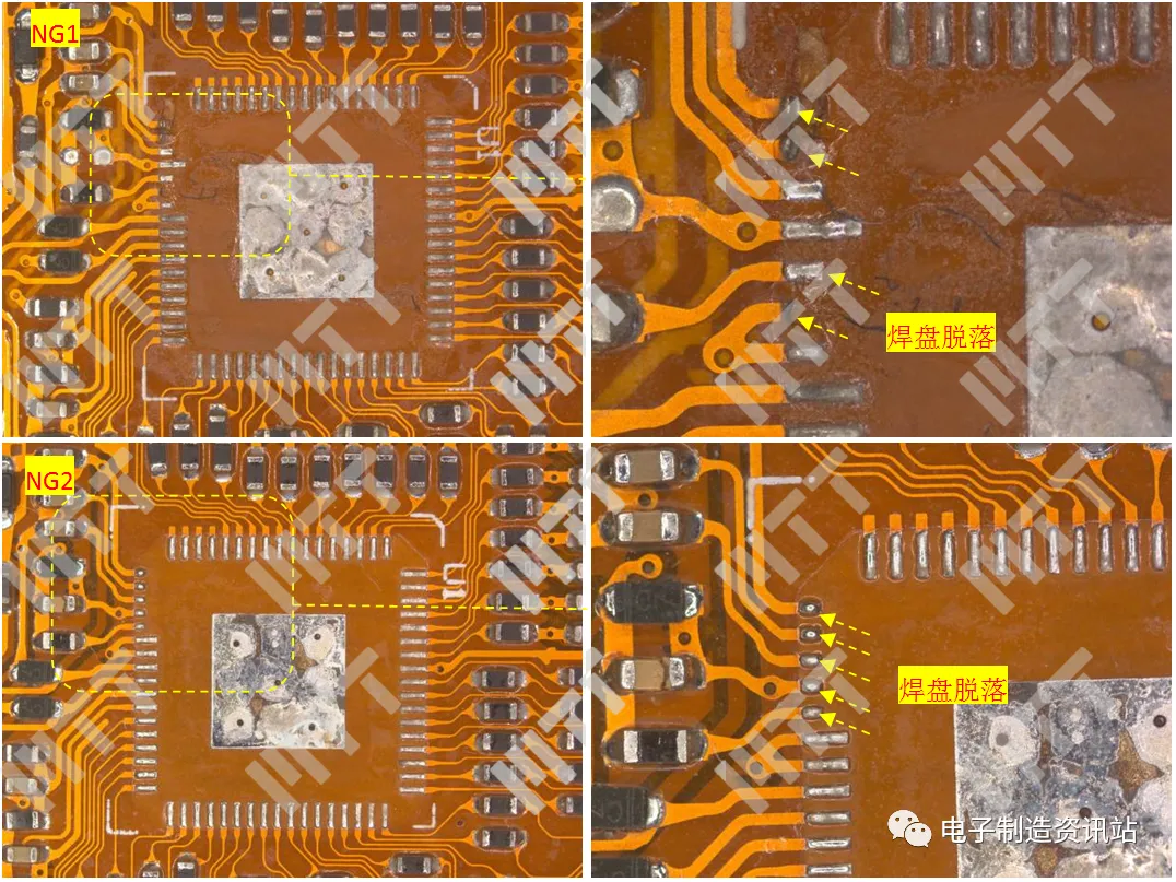
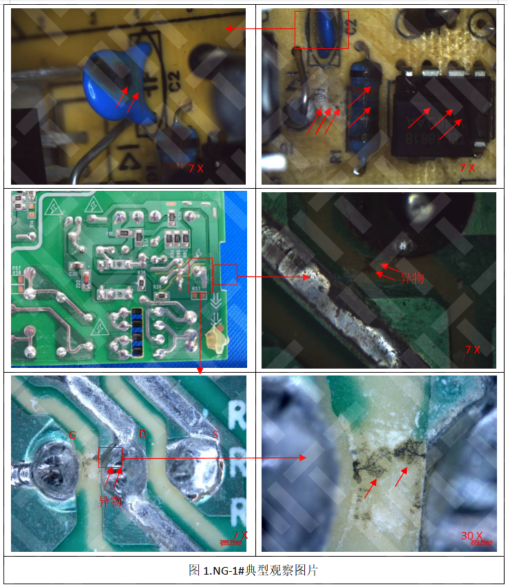
1. Appearance inspection
NG1, NG2 samples in the same corner of the QFN chip found that the pad shedding phenomenon, the other three corners of the position of the pad did not see a significant shedding phenomenon, the failure phenomenon and the client feedback information is consistent.
Figure 1. FPC appearance inspection typical photos
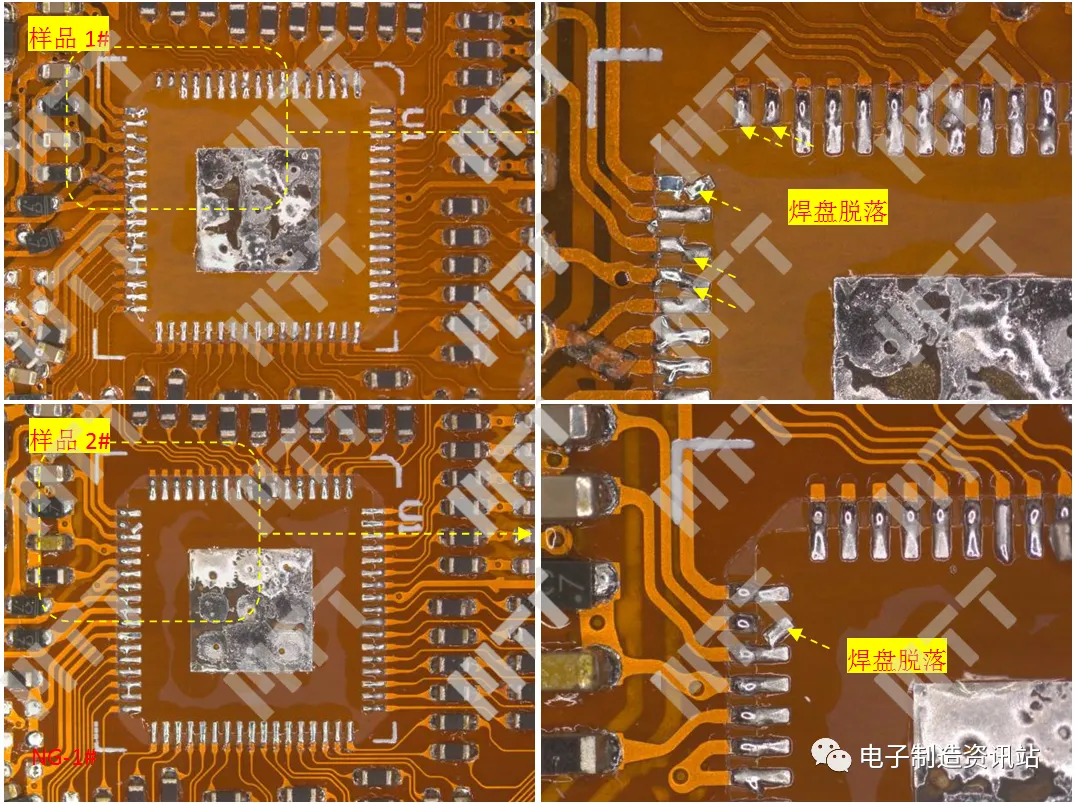
2. Simulation verification
In order to confirm that the FPC finished product welding process does indeed have a pad shedding abnormality, from the FPC finished product randomly selected 2pcs for dewelding treatment, the results found that the sample has a pad shedding abnormality (named sample 1#, sample 2#), the result is shown in Figure 2.
Sample 1#, 2# in the same corner of the QFN chip are found in the same corner of the pad fallout phenomenon, the pad shedding position and the failure sample performance is consistent, so FPC finished product after the welding of the plate does exist abnormality.
Figure 2. Sample 1#, 2# shedding pad appearance inspection photos
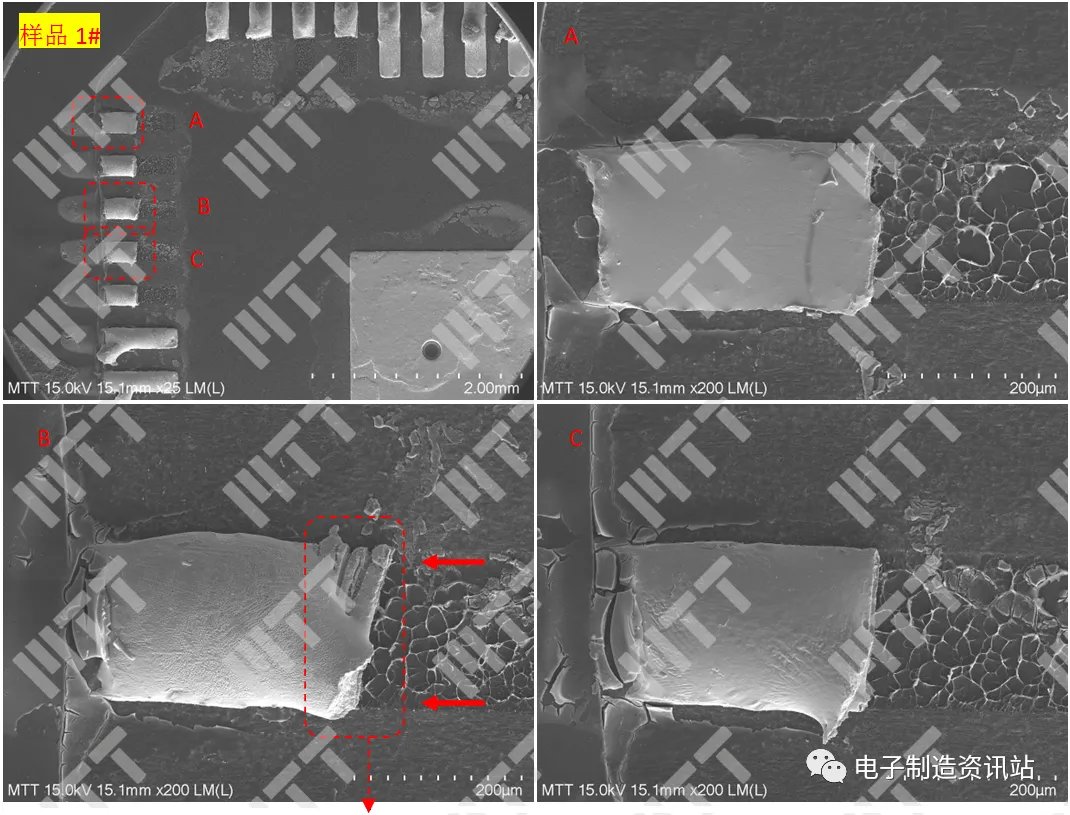
3. Surface analysis
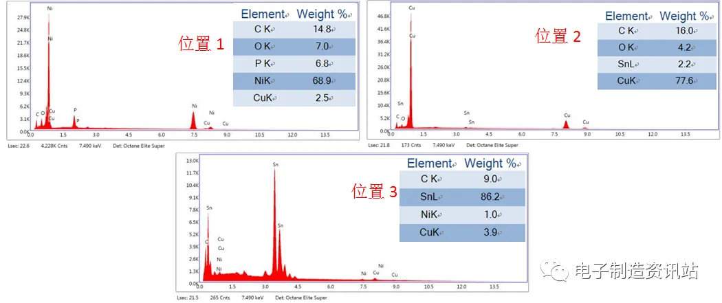
The results of morphological observation and composition analysis show that all shedding pads are separated from the same position, and the break shows the characteristics of force deformation. The EDS test results showed that no significant abnormal elements were found at the breakout position.
Figure 3. Sample 1# the position of the pad morphology observation photo and composition test results
4. Profile analysis
In order to confirm the presence of defects in the same batch of FPC finished product pads, the 2pcs sample was randomly selected from the remaining FPC finished product for slicing analysis, and it was found that the 2pcs sample (named finished product 1, finished product 2) was abnormally disconnected from the cutter, and the results were as follows:
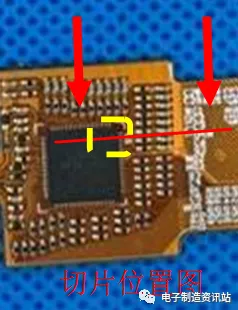
Figure 4. FPC sample slicing position diagram
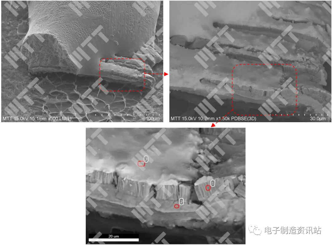
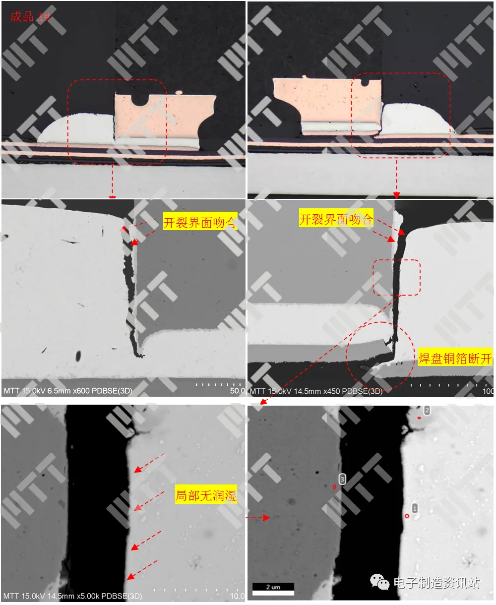
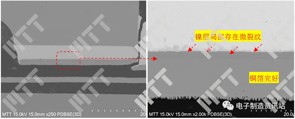
Finish 1: as shown in Figure 5, after the slice, a pin pad (Figure 4 yellow box position) is obviously found to disconnect abnormal, another pin solder joint local cracking, disconnected interface matching, showing obvious force fracture characteristics; disconnection interface local presence of no wetting phenomenon, poor interface wetting will lead to the interface welding strength reduction; solder breakout around the copper foil intact, nickel layer local discovery of micro-cracks phenomenon.
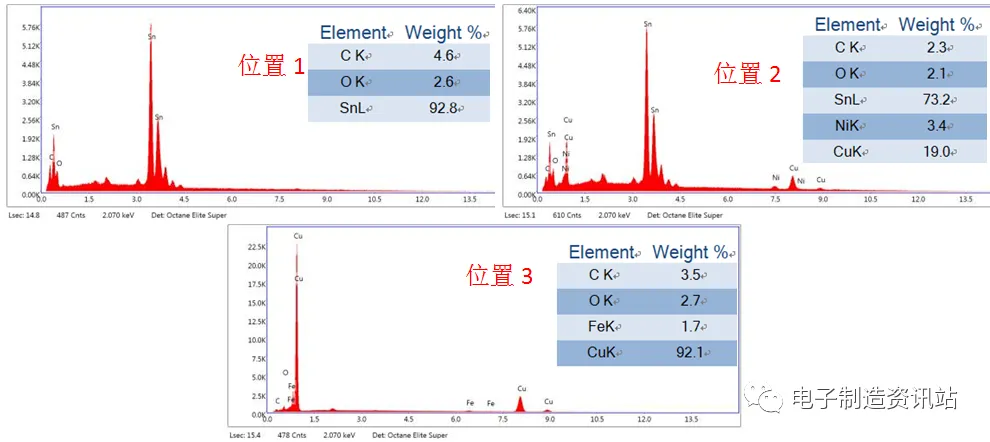
Figure 5. Sample 1 after the finished product 1 sample is sliced and the pin solder joint cross-section metallographic observation photo and SEM+EDS analysis results
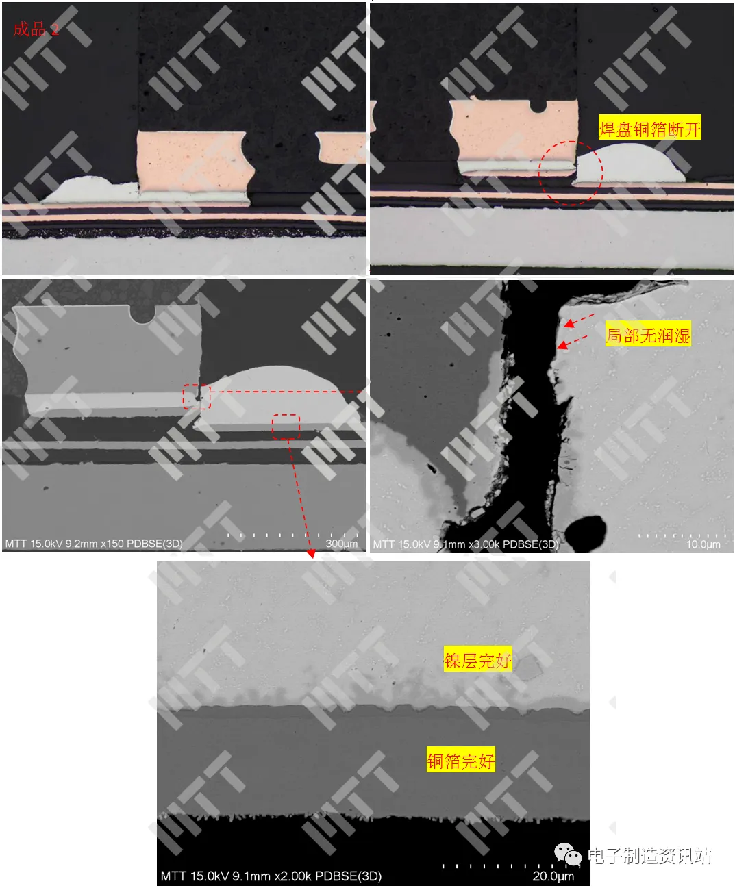
Finished 2: as shown in Figure 6, after slicing, the yellow box position pins in Figure 4 are also found to disconnect abnormally, disconnect the interface is consistent, showing obvious force fracture characteristics; disconnection interface local presence of no wetting phenomenon, poor interface wetting will lead to a reduction in the welding strength at the interface; the copper foil and nickel layer around the cutter break are intact, indicating that the electrode disconnection abnormality is not directly related to the micro-splitting of the plate nickel layer.
Figure 6. Finish 2 sample slicing after the pin solder joint cross-section metallographic observation and SEM morphology observation photo
The above results can be seen that the reason for the disconnection of the pad is that after the welding is formed, the QFN solder joint is affected by external forces, resulting in the welding joint being disconnected along the weak position of the welding strength (the breaking interface wetting bad position), which eventually leads to the break of the pad.
5. Analysis and discussion
The background of the failure in this case is: the problem of pad shedding during the repair process after FPC assembly.
The appearance inspection of the solder plate shedding sample found that the pad shedding occurred in the same corner position of the QFN chip, and the other three corners of the pad did not see the obvious weld plate shedding phenomenon.
In order to confirm that the QFN device heating and dewelding process, there is indeed an abnormality in the pad shedding, and the same batch of FPC finished products are unweldified with the help of the heating table (set 250 ° C). The results show that in the process of welding individual FPC finished products, there is indeed a phenomenon of pad shedding.
The morphological observation and composition analysis of the sample after the welding plate shedding. The results show that all the shedding pads are removed from the same position, the break shows the deformity of the force, and the disconnect position does not find obvious abnormal elements.
In order to confirm the defects in the solder pad of the finished batch of FPC products, the sliced analysis of the QFN pin solder joint on the finished FPC showed that:
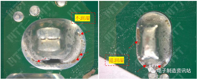
More than 1 sample QFN in the same corner position of the solder joints are found to disconnect abnormal, disconnect the interface is consistent, disconnected position pad is pulled off, showing obvious force fracture characteristics;
There is no wet phenomenon in the local position of the disconnected interface, and the poor wetting of the interface will lead to a reduction in the welding strength of the interface;
3, the copper foil around the break of the pad is intact, individual shedding of the pad nickel layer found micro-cracks phenomenon, nickel layer micro-cracks and pad shedding no obvious correlation.
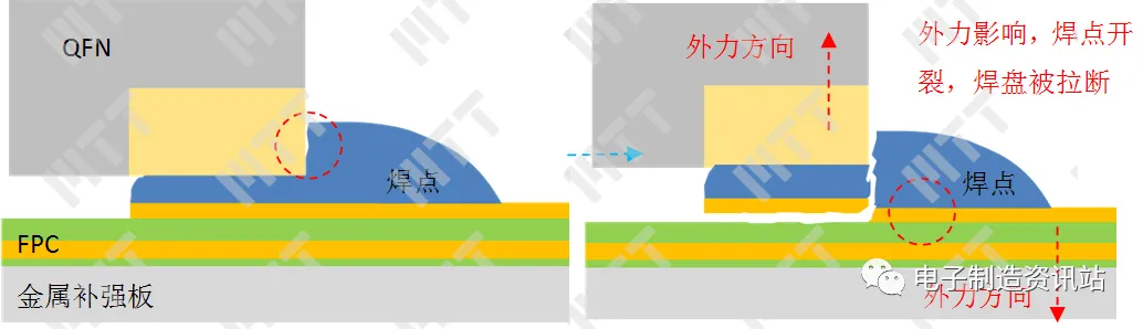
In summary, the FPC pad disconnection process is shown in Figure 7, after the QFN device reflow welding, the pin solder joint local wetting phenomenon, resulting in a reduction in the welding strength of the interface, under the action of a larger external force, the welding joint along the weak welding strength began to crack, and eventually led to the welding disc being pulled off.
Figure 7. QFN device pin solder spot pad disconnection process diagram
6. Summary and recommendations
Summary: The reason for FPC pad shedding is that after reflow welding, the solder joint is affected by a large external force, which causes the solder joint to crack in a weak position along the welding strength, and eventually leads to the break of the pad.
Recommendation: After welding, check the sample force of each station to prevent greater external forces acting on the surface of the product.


Maxin Testing Laboratory
Learn more about our company

Electronic Manufacturing Information Hub
See more exciting case studies

Video Channel
Watch more exciting videos


 Buildings A1, A3, and A5, Peking University Science and Innovation Park, Songbai Road, Bao'an District, ShenzhenBuilding 3, Xinyao Valley, 415 Changyang Street, Suzhou Industrial Park, Suzhou City1st Floor, Building 4, No. 39 Anzhi Street, Suzhou Industrial Park, Suzhou City