+86-400-850-4050


Didn't find what you were looking for?
Consult a professional engineer immediately for your service


After the aging test, a product found that the standby working current is abnormally increased. After detailed analysis, it was determined that the problem stemmed from the abnormality of the C6 capacitor (the capacitor of the specific position or function on the circuit board). In order to comprehensively and deeply explore the root cause of C6 capacitance failure, we have adopted a series of professional and systematic detection methods to carry out failure analysis work.
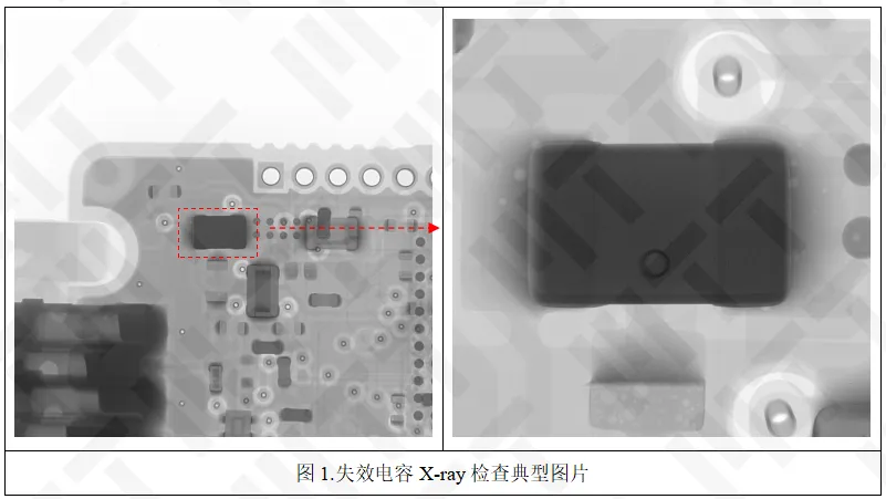
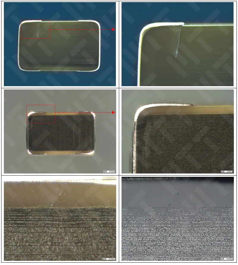
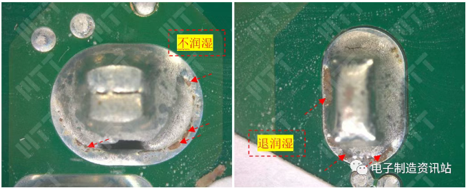
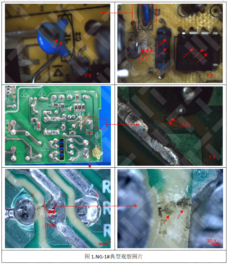
1. Appearance Check & X-ray Perspective The
surface of the failed capacitor capacitor does not find obvious cracks,
damage and other abnormal phenomena, excluding the failure caused by
factors such as external force impact of the capacitor. Use X-ray to
perform perspective inspection of the failure capacitor, and no obvious
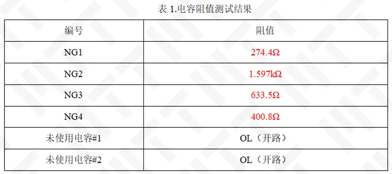
structural abnormalities were found. 2. Electrical Parameter Testing The
failure capacitance resistance is less than 2kΩ, which is much less
than the unused capacitance resistance, indicating that the failure
capacitor has obvious leakage phenomenon, as shown in Table 1 of the
test result.
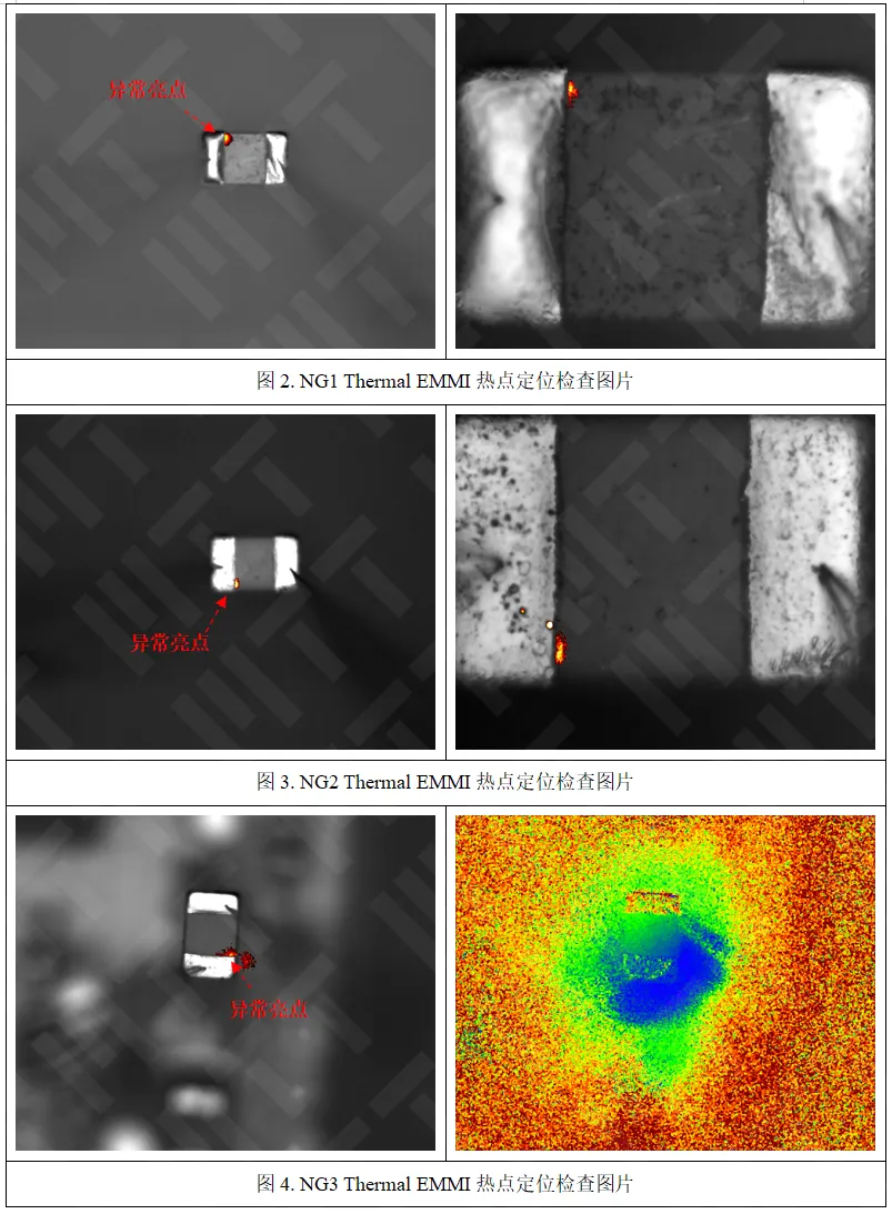
3. Thermal EMMI Hotspot Positioning It
was found that there are obvious abnormal highlights inside the failure
capacitor, and the highlights are mainly concentrated on the side of
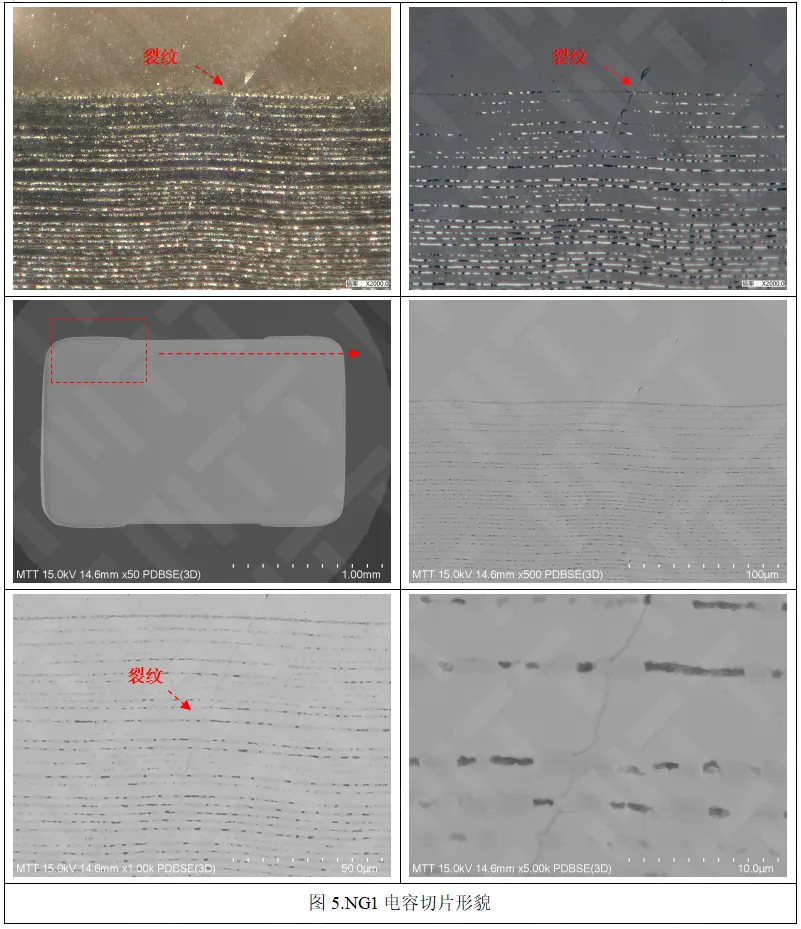
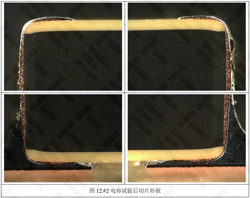
the electrode near the capacitance end. 4. Sliced analysis (1)
The position where the NG1 capacitor shows abnormal bright spots in the
hot spot has obvious cracks. Further grinding to the inner electrode is
revealed, and the crack is found to pass through the intersection of
the inner electrode, resulting in a short circuit or low resistance
channel between the upper and lower layers of the inner electrode.
Compared with the slicing of different locations, with the gradual
grinding to the inside of the capacitor, the cracks gradually become
smaller, indicating that the origin of the crack expansion should be
close to the outside of the capacitor. In addition, the microscopic
morphology observes that the cracks are fine, and no melting and burning
phenomenon is seen, which is presumed to be mechanical stress cracks. (2)
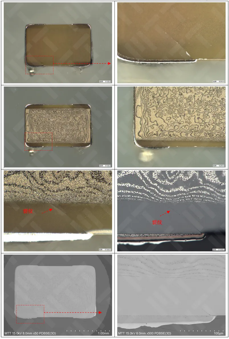
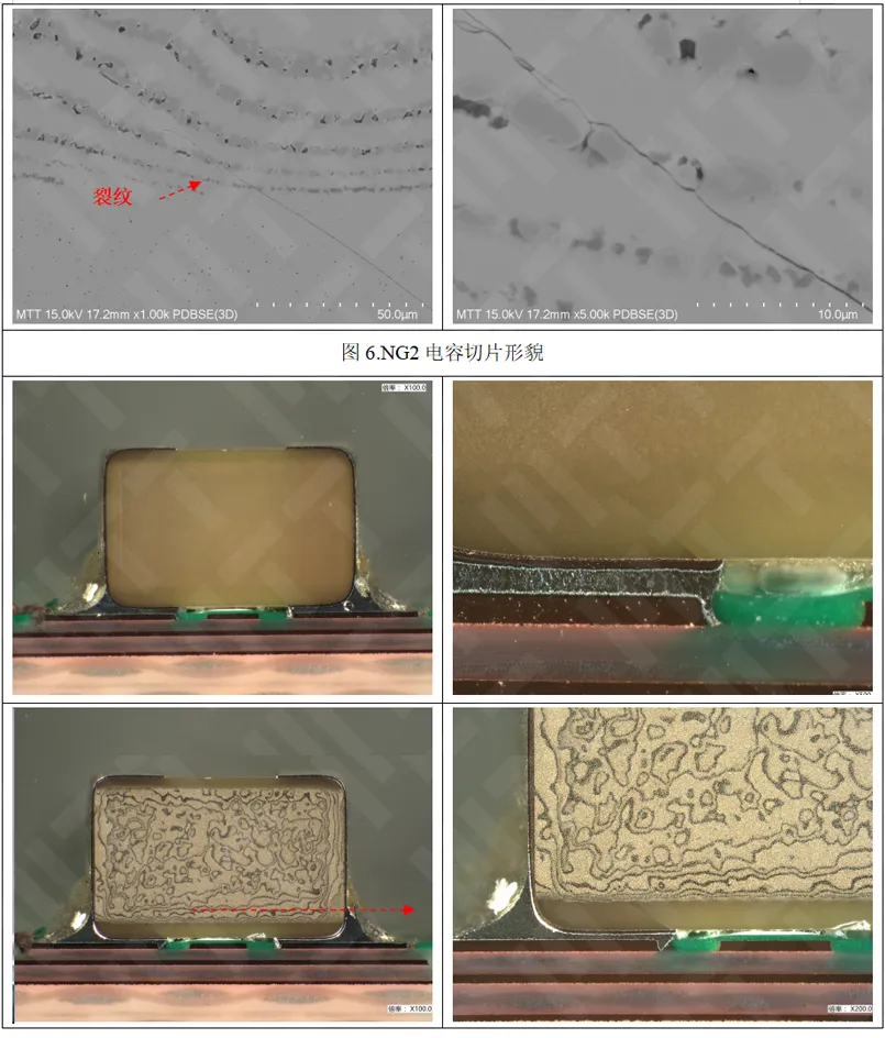
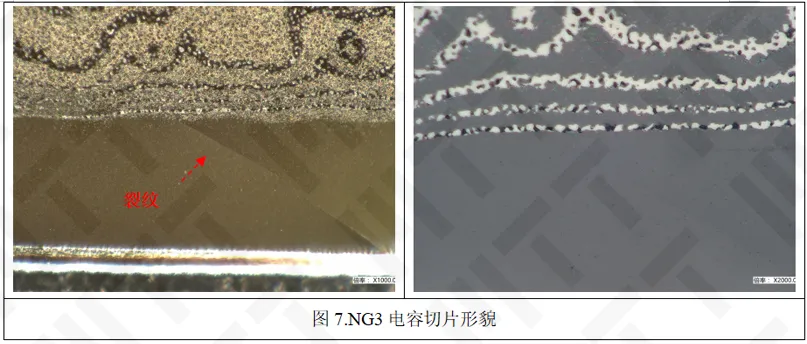
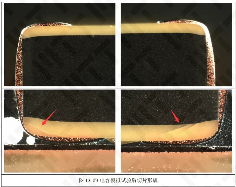
NG2, NG3 are found on the bottom side of the capacitor crack, and
extended to the inner electrode area to cause the capacitor layer
between the leakage short circuit, the position and hot spot abnormal
bright spot corresponding. The crack originated from the bottom surface
end electrode, and its angle and the bottom angle is close to 45 °,
which is a typical mechanical stress cracking morphology.
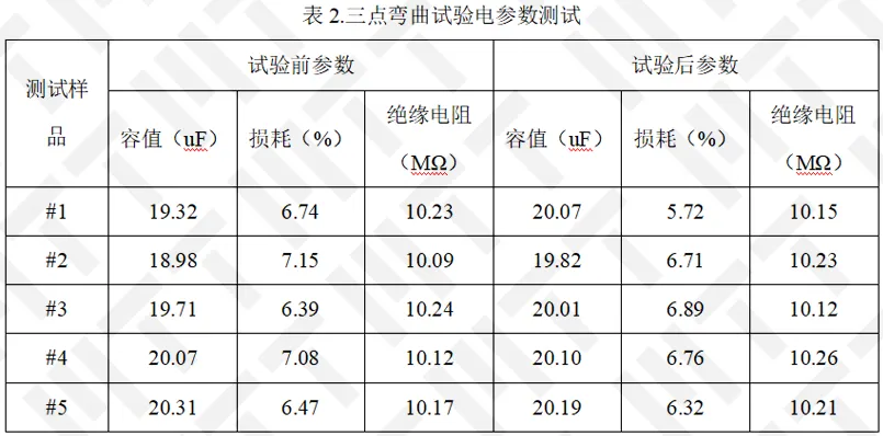
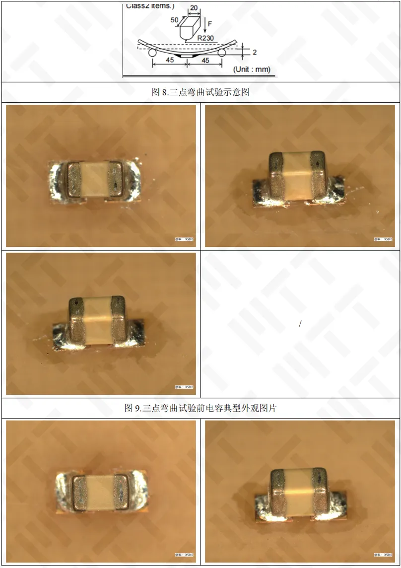
5. Material verification According
to the specification book, the three-point bending test is carried out
to confirm the appearance and electricality of the capacitor after the
experiment, and no obvious abnormalities are found. The slice analysis
of #1 and #2 capacitors has not been found to have obvious cracks,
medium layer holes and other defects. Therefore, the material can meet
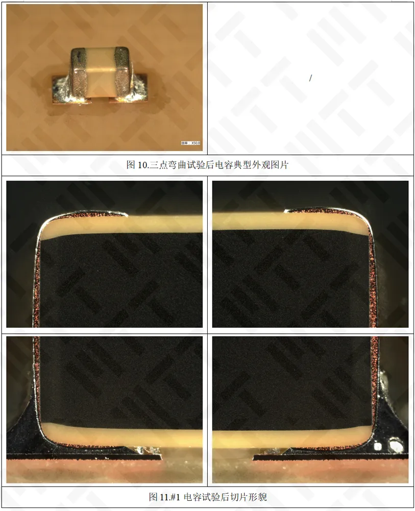
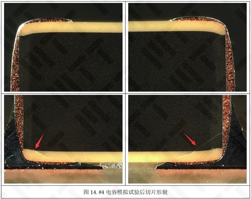
its specifications. 6. Simulation experiment In
order to confirm whether the internal crack of the failure capacitor is
a mechanical stress crack, the #3 and #4 capacitors continue to bend
simulation test for the three-point bending, and the capacitance is
slicing analysis after the test. The
slicing results show that when the substrate is bent at 4mm, there are
obvious cracks in the interior of the #3 and #4 capacitors, and its
position originates from the end electrode position and is 45° with the
welding surface, which is basically the same as the internal cracking
morphology characteristics of the failure capacitor. Therefore, it is
inferred that the failure capacitor is subjected to a large external
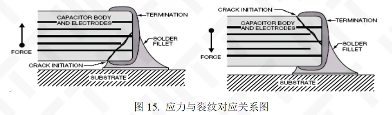
stress, and then cracks occur internally. 7. Analysis and Summary Analysis:
The reason for the mechanical stress crack inside the capacitor is that
because the capacitive porcelain body is made of hard and brittle
ceramic material, this material is more sensitive to the stress
generated by the deformation of the single plate. When the capacitor is
subjected to additional stress, the crack will be generated at the
stress concentration point, as shown in Figure 15, if the device is
subjected to upward stress, the bottom weld end and the welding end of
the intersection at the junction of the welding end is the stress
concentration point, this position becomes a weak link, easy to produce a
crack with the welding end of 45° or "Y" font, and vice versa. Summary:
The main reason for the failure of the capacitor is that the cracks
that are extended to the inter-internetized electrode by external stress
are formed, resulting in a decrease in the resistance value caused by
the leakage channel. 8. Recommendation Check the external stress sources in the process of capacitance assembly, testing, etc.


Maxin Testing Laboratory
Learn more about our company

Electronic Manufacturing Information Hub
See more exciting case studies

Video Channel
Watch more exciting videos


 Buildings A1, A3, and A5, Peking University Science and Innovation Park, Songbai Road, Bao'an District, ShenzhenBuilding 3, Xinyao Valley, 415 Changyang Street, Suzhou Industrial Park, Suzhou City1st Floor, Building 4, No. 39 Anzhi Street, Suzhou Industrial Park, Suzhou City