+86-400-850-4050


Didn't find what you were looking for?
Consult a professional engineer immediately for your service


After a PCBA patch, the hot pressure welded end wire is lightly pulled off, and the capacitor/resistance component will also drop slightly. The unwelded same batch of SET board has tin undesirable. A series of test analyses of 3pcs failure samples are now being carried out to find the root cause of poor PCBA solder joint welding.
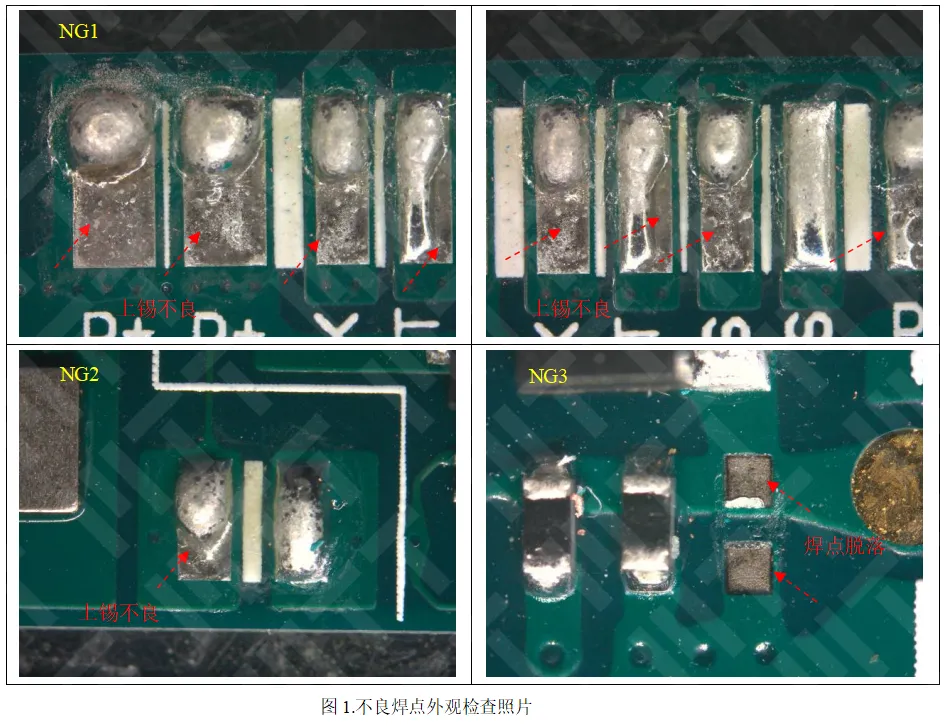
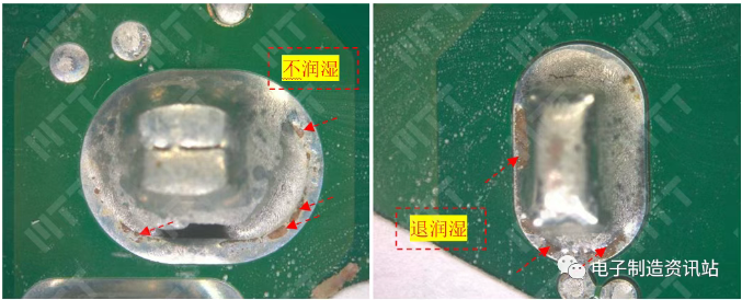
1. Appearance inspection
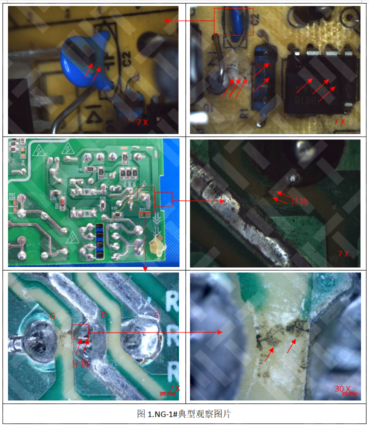
Choose 3 typical bad solder joints, optical inspection, the results are shown in Figure 1: most of the bad solder joints surface of the obvious wettling phenomenon, the color of the pads is blacked abnormal, the individual solder joints are removed, and the side of the welding disc is black.
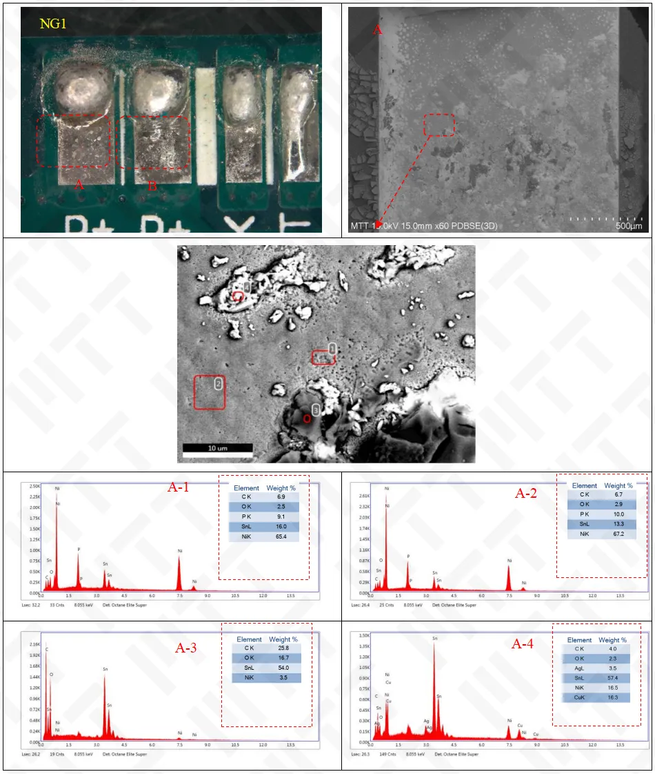
2. Surface analysis
NG1: As shown in Figure 2, the surface of the damp rod wets the poor position, and the local presence of solder and flux residues; the wet surface contains C, O, P, Sn, Ni, Ni elements, the residual position of the solder contains C, O, Ag, Sn, Ni, Cu elements, and the residual position of the flux contains C, O, Sn, Ni elements, and no abnormal elements exist.
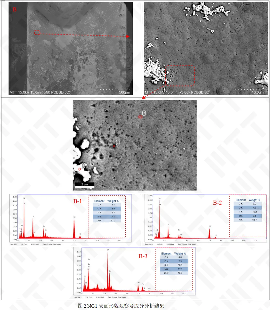
NG2, NG3: Wetting bad position morphology is similar to NG1, the composition contains C, O, P, Sn, Ni elements, no abnormal elements exist.
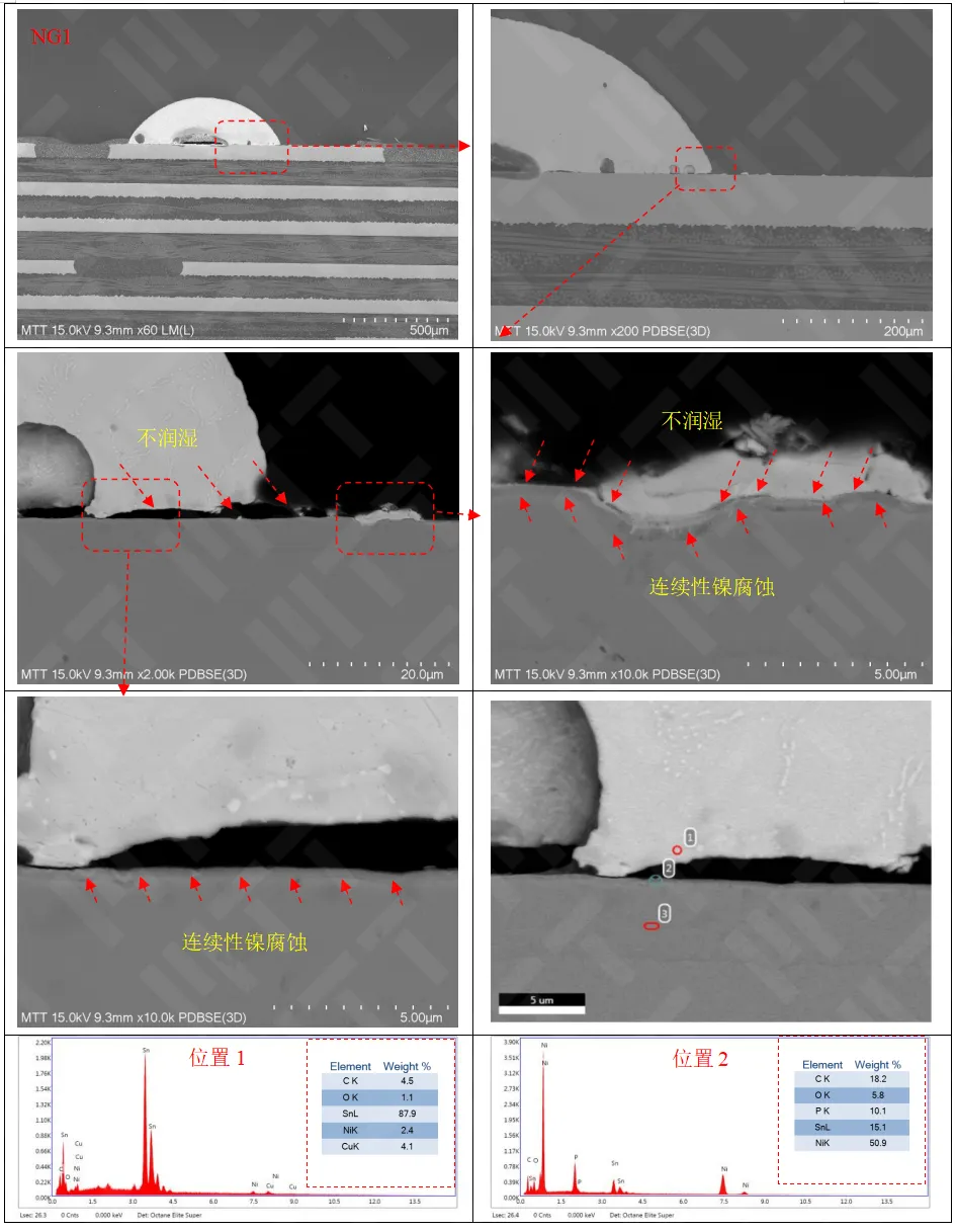
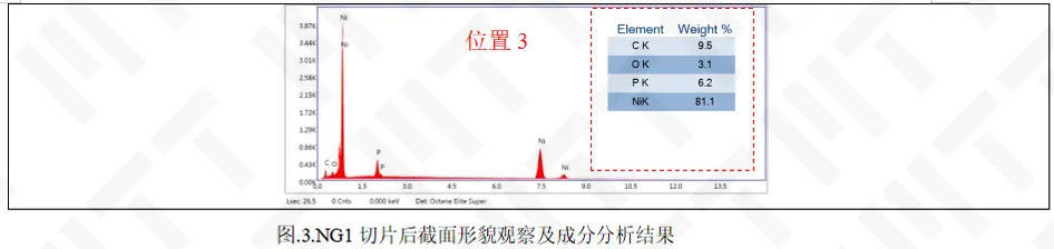
3. Profile analysis
NG1: As shown in Figure 3, the slicing results show: after the bad solder plate slice, the solder residue position and no residual position are found to be non-wetting phenomenon; after amplification observation, there is a significant continuous nickel corrosion abnormality in the non-wetting position; Ni layer P content is 6.2wt%.
NG2, NG3: The slicing results are similar to the NG1 result, and the continuous nickel corrosion anomalies are also found in the non-wetting position.
4. Analysis and Summary
To sum up: PCBA solder joint welding bad reasons are mainly related to the continuous Ni layer corrosion, Ni layer corrosion, welding process, Au layer quickly melted in the solder, and as the welding substrate of the Ni layer can not form an effective metallurgical combination with the solder, that is, IMC layer, ultimately leading to the occurrence of welding spot wetting.
Ni layer corrosion is mainly due to the excessive oxidation of the surface of the nickel layer during the immersion of the PCB pad. The irregular deposition of large gold atoms and their rough grain is sparsely porous, resulting in the continuous "Galvanic effect" of the underlying nickel layer, which in turn causes the nickel layer to continuously oxidize, resulting in the continuous accumulation of undissolved nickel rust under the gold surface.
Summary: The cause of PCBA solder joint welding is mainly related to the continuous nickel corrosion of the PCB pad Ni layer, which causes the base Ni layer to be unable to form an effective metallurgical combination with the solder, that is, the IMC layer, which eventually leads to the occurrence of poor wetting of the solder.
5. Recommendation
Increase the quality control of PCB materials, such as weldability verification tests, to avoid the flow of abnormal materials into production.


Maxin Testing Laboratory
Learn more about our company

Electronic Manufacturing Information Hub
See more exciting case studies

Video Channel
Watch more exciting videos


 Buildings A1, A3, and A5, Peking University Science and Innovation Park, Songbai Road, Bao'an District, ShenzhenBuilding 3, Xinyao Valley, 415 Changyang Street, Suzhou Industrial Park, Suzhou City1st Floor, Building 4, No. 39 Anzhi Street, Suzhou Industrial Park, Suzhou City