+86-400-850-4050


Didn't find what you were looking for?
Consult a professional engineer immediately for your service


As a new generation of power semiconductor devices, SiC half-bridge modules play an important role in the power electronics industry. It significantly improves the performance of the power conversion system with high pressure resistance, low loss and high efficiency. In the fields of new energy vehicles, photovoltaics, and energy storage, the application of SiC half-bridge modules has effectively reduced energy consumption and improved system efficiency and reliability.
A SiC half-bridge module fails after testing, the gate resistance is abnormally reduced (10Ω/30Ω, normal is infinite), and the DS end is short circuit. Now, the failure analysis of 2 OK modules of the 3pcs NG module is performed to find the cause of its failure.
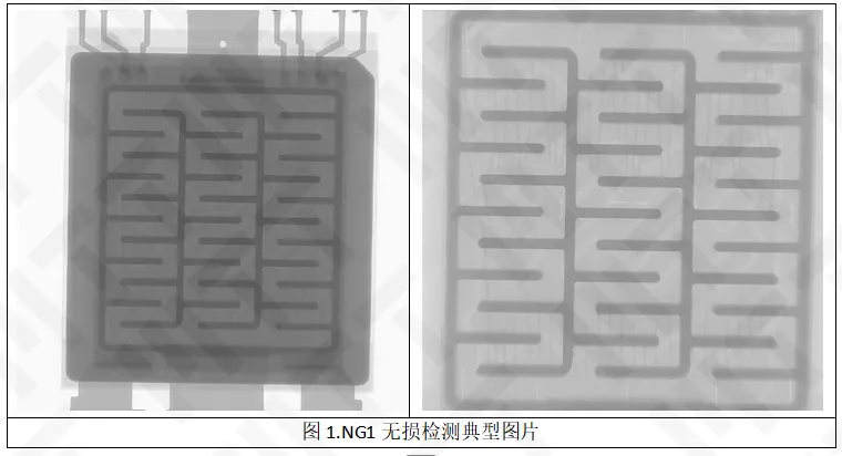
1. Appearance & Nondestructive Testing
All modules do not find cracking, deformation, charred anomalies. Silk printing model and other information has traces of polishing, pins have solder residue, there are traces of deintered welding. The results of the 3pcs NG module for perspective inspection showed that the non-destructive testing of the 3pcs NG module did not find the bonding broken and cross-cutting phenomenon, and no obvious burning phenomenon was found inside.
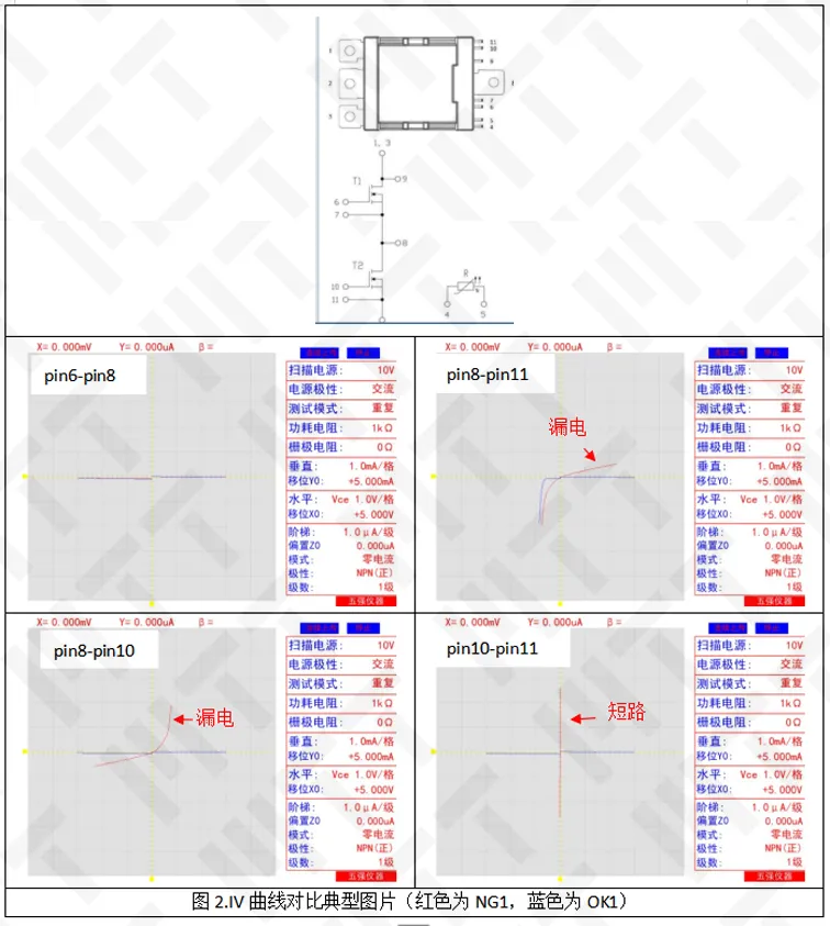
2. The IV curve
The NG module consists of two upper and lower MOS (T1 and T2), where the lower MOS tube (T2) is obviously abnormal.。
NG1/NG2: under the MOS tube G-S very short circuit, D-S extreme leakage;
NG 3: Under MOS tube G-D-S pole two short circuit.
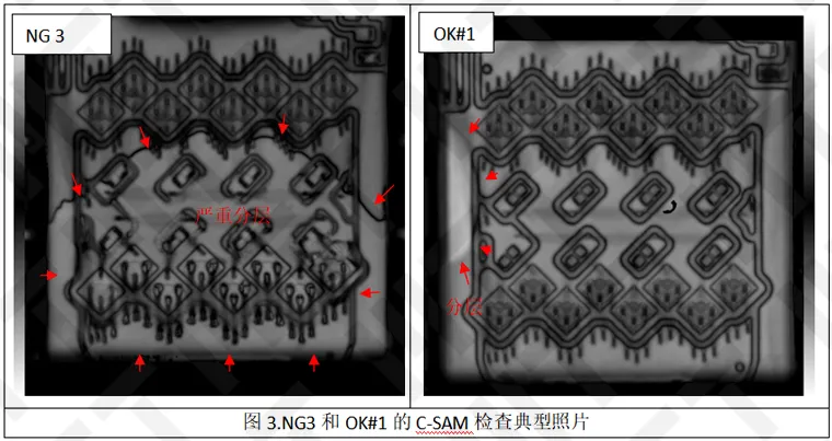
3. C-SAM testing
It was found that there was a serious stratification of the MOS area under NG3, and combined with electrical characteristics, NG3 should have been severely burned. Other failure modules and normal modules have no layering anomalies, and only the OK1 module C-SAM inspection finds that the edge position of the substrate is layered.
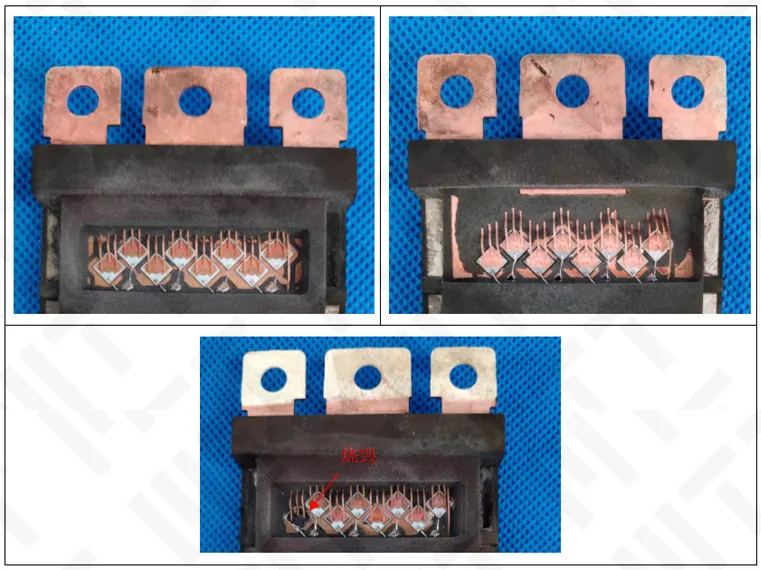
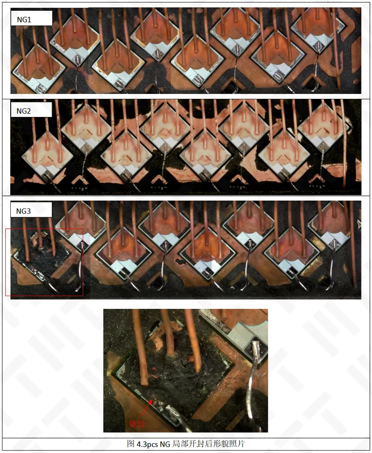
4. Opened
NG3 found that the leftmost chip in the MOS tube chipset burned severely. From the burning morphology analysis to overflow heat to burning. NG1 and NG2 did not find that the MOS chipset was significantly burned.
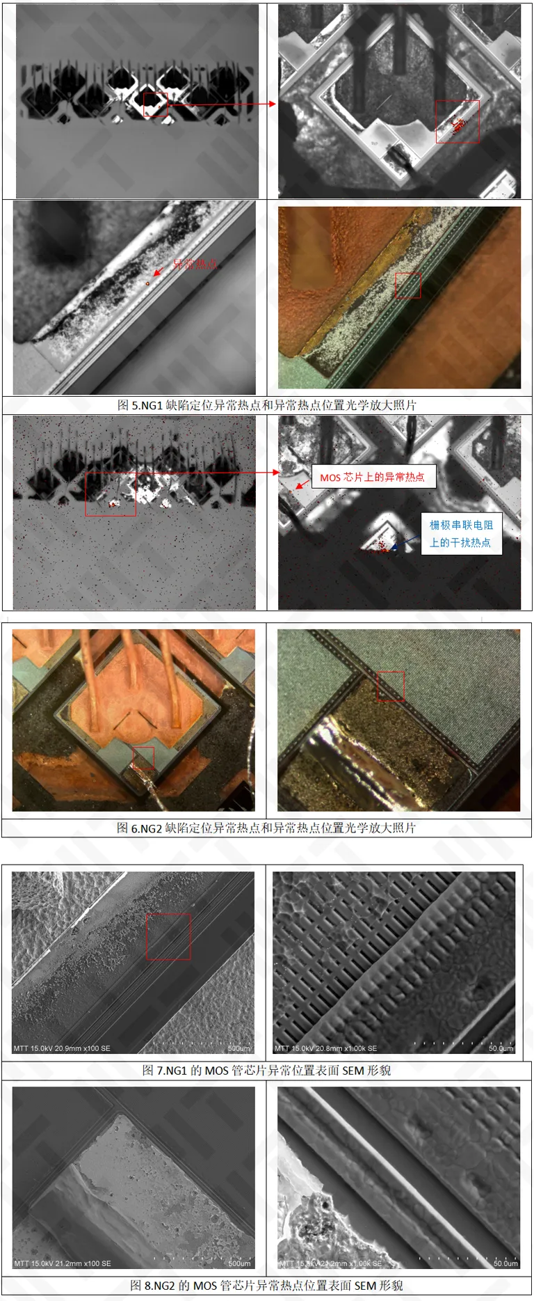
5. Defect Positioning & Microanalysis
After the opening of the open did not find the obvious burned NG1 and NG2 defect positioning, found:
The NG1 defect positioning shows anomalous hot spots on the fifth MOS chip from left.
The NG2 defect positioning shows that there are abnormal hot spots on the third MOS chip from left, and interference hot spots on the gate series circuit.
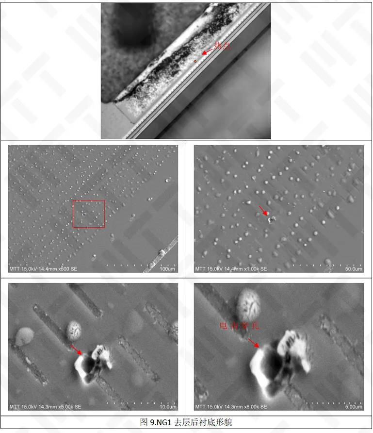
The optical/SEM observed the abnormal hot spot position of the MOS chip NG1 and NG2, and no obvious abnormalities were found.
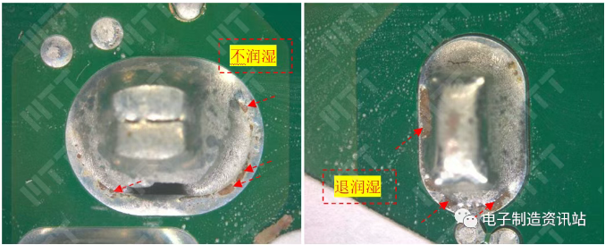
6. Delayer observation (take NG1 as an example)
NG1 and NG2 MOS chip abnormal hot spot surface is not found to be obvious abnormal, so it is necessary to observe the substrate. NG1 and NG2 failure mode is the same, are due to the gate overvoltage caused by breakdown, so NG1 as an example for detailed analysis.
The picture shows that NG1 has an electroshock perforation on the position of the anomalous hot spot on the back of the delayer.
From the above, it can be seen that the short circuit between the GS of the MOS under NG1 is due to the electric breakdown of the gate medium layer. Because the gate of the MOS tube is sensitive to overvoltage, it is inferred that NG1 and NG2 are due to overvoltage in the lower MOS gate. This overvoltage may be an ESD or an abnormal surge voltage.
7. Summary
A chip in the MOS tube under NG3 fails short-circuited G, D, and S due to overcurrent heat.
MOS under NG1 and NG2 fail for short-circuited by gate overvoltage breakdown.
8. Recommendation
1) For the overcurrent heat burning, the need to improve heat dissipation;
2) For gate overvoltage breakdown, it is recommended to do ESD protection and gate surge voltage suppression.


Maxin Testing Laboratory
Learn more about our company

Electronic Manufacturing Information Hub
See more exciting case studies

Video Channel
Watch more exciting videos


 Buildings A1, A3, and A5, Peking University Science and Innovation Park, Songbai Road, Bao'an District, ShenzhenBuilding 3, Xinyao Valley, 415 Changyang Street, Suzhou Industrial Park, Suzhou City1st Floor, Building 4, No. 39 Anzhi Street, Suzhou Industrial Park, Suzhou City