+86-400-850-4050





Didn't find what you were looking for?
Consult a professional engineer immediately for your service
























Click on Blue.
Care for us
In highly integrated electronics, micron-scale solder joint cracks or nano-scale electrochemical migration can cause systemic failures and cause significant economic losses. Failure analysis has evolved from the traditional "after-the-fact attribution" to the core engine of "full life cycle quality control", as the core means of product quality assurance, and cracked the failure mechanism through reverse engineering, providing a scientific basis for process optimization and reliability design.
This paper will systematically explain the electronic process failure analysis technology system, combined with the typical scene depth analysis of technical logic, to build a systematic solution from failure prevention to root cause governance.
01
Core Values of Failure Analysis:
From Passive Response to Active Defense
The value of failure analysis far exceeds the problem solving itself, and the role of product quality is reflected in:
Defect traceability: Precise positioning design defects (such as BGA layout mismatch), process abnormalities (such as electroplating pollution), material degradation (such as CAF migration) and other failure root causes;
Risk prediction: Establish a threshold model for critical parameters through the Failure Mode Database (FMEA) to achieve early warning of potential failures.
Cost optimization: Avoid waste of resources caused by blind improvement and reduce the cost of enterprise quality;
Technology iteration: Promote the upgrading of process standards and the introduction of new materials.
02
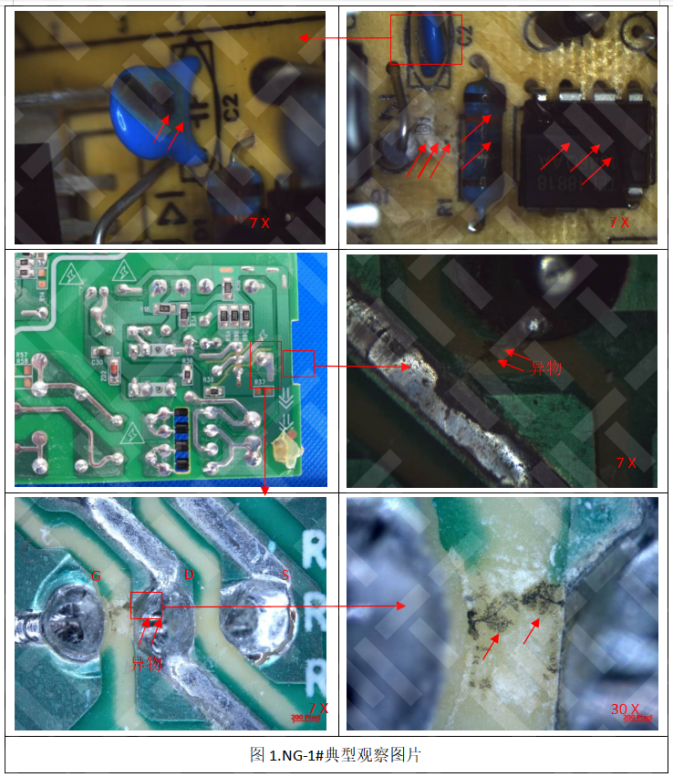
Typical failure analysis of electronic products
The early stage of determining the cause of failure is so as to initially determine the possible cause of failure and follow-up analysis direction
Failure analysis and analysis process follows the principle "non-destructive → micro-loss → destruction"
03
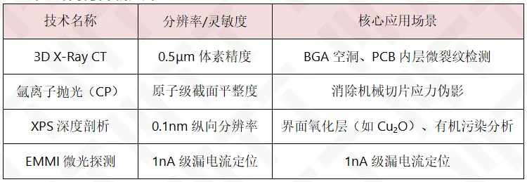
Application of advanced analysis technology
04
Common failure of electronic products &
Definition of Common Terminology
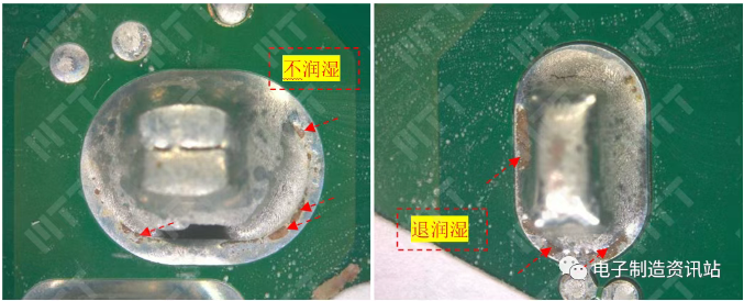
Common failure: bad tin on the PCB pad, PCB burst plate layering, PCB through hole abnormalities (open circuit or resistance), poor BGA function (pillowing effect, etc.), device solder joint shedding, solder joint cracking or corrosion, etc.
Definition of Common Terminology:
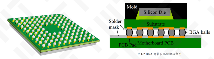
1. Ball Grid Array (BGA): The terminal flange is arranged in a raster form a surface mount package at the bottom of the package.
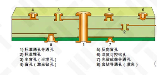
2. Blind hole: extends only to the conduction hole on one surface of the printed board.
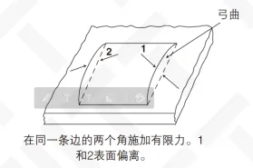
3. Bow (complete board, board or printed board): A shape of the board relative to the plane, can be roughly represented by cylindrical or spherical curvature. If the product is rectangular, the corner of the board falls on a plane.
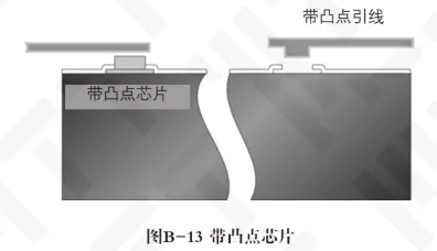
4. convex (chip): The chip connects the metal protrusion part of the disk or the belt for internal lead bonding.
5. With convex chip: A semiconductor chip with a metal protrusion section for internal lead bonding.
05
In-depth disassembly of typical electronic process cases:
Full technical details are available.
BGA solder joint tin - precise sniping of thermal stress deformation
Background: A certain proportion of the tin failure in the assembly of a certain model of BGA, and the position of the tin is relatively fixed. Failure ratio: 0.06%. PCB surface treatment OSP.
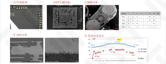
CT scan analysis : The failure sample is found to be tin in the corner of the fixed diagonal, and the edge of the edge position in this diagonal direction is significantly smaller than the other direction.
Profile analysis: The failure sample and the normal sample are low and intermediate high on both sides of the solder joint height in the diagonal direction, and the deformation of the diagonal direction is more serious, so the tin failure is directly related to the degree of deformation during the PCBA welding process.
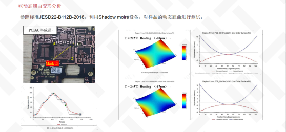
Dynamic warping test: PCBA semi-finished products in the welding process as a whole decontamination, and the failure diagonal direction of concave deformation is more obvious, and the actual deformation trend after welding is consistent.
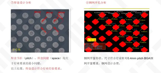
Welding plate and steel mesh size measurement: The pad and steel mesh design is reasonable and meets the industry design requirements.
Summary: The root cause of the BGA in the relatively fixed position of the tin: PCBA semi-finished products (first-sided reflow welding) welding process in the fixed diagonal direction of a large degree of concave deformation, resulting in corner position welding joints are extruded and tin.
Pay attention to us and get more in-depth analysis of materials science!







Maxin Testing Laboratory
Learn more about our company

Electronic Manufacturing Information Hub
See more exciting case studies

Video Channel
Watch more exciting videos









 Buildings A1, A3, and A5, Peking University Science and Innovation Park, Songbai Road, Bao'an District, ShenzhenBuilding 3, Xinyao Valley, 415 Changyang Street, Suzhou Industrial Park, Suzhou City1st Floor, Building 4, No. 39 Anzhi Street, Suzhou Industrial Park, Suzhou City